Applications information – Rainbow Electronics MAX1249 User Manual
Page 13
MAX1248/MAX1249
+2.7V to +5.25V, Low-Power, 4-Channel,
Serial 10-Bit ADCs in QSOP-16
______________________________________________________________________________________
13
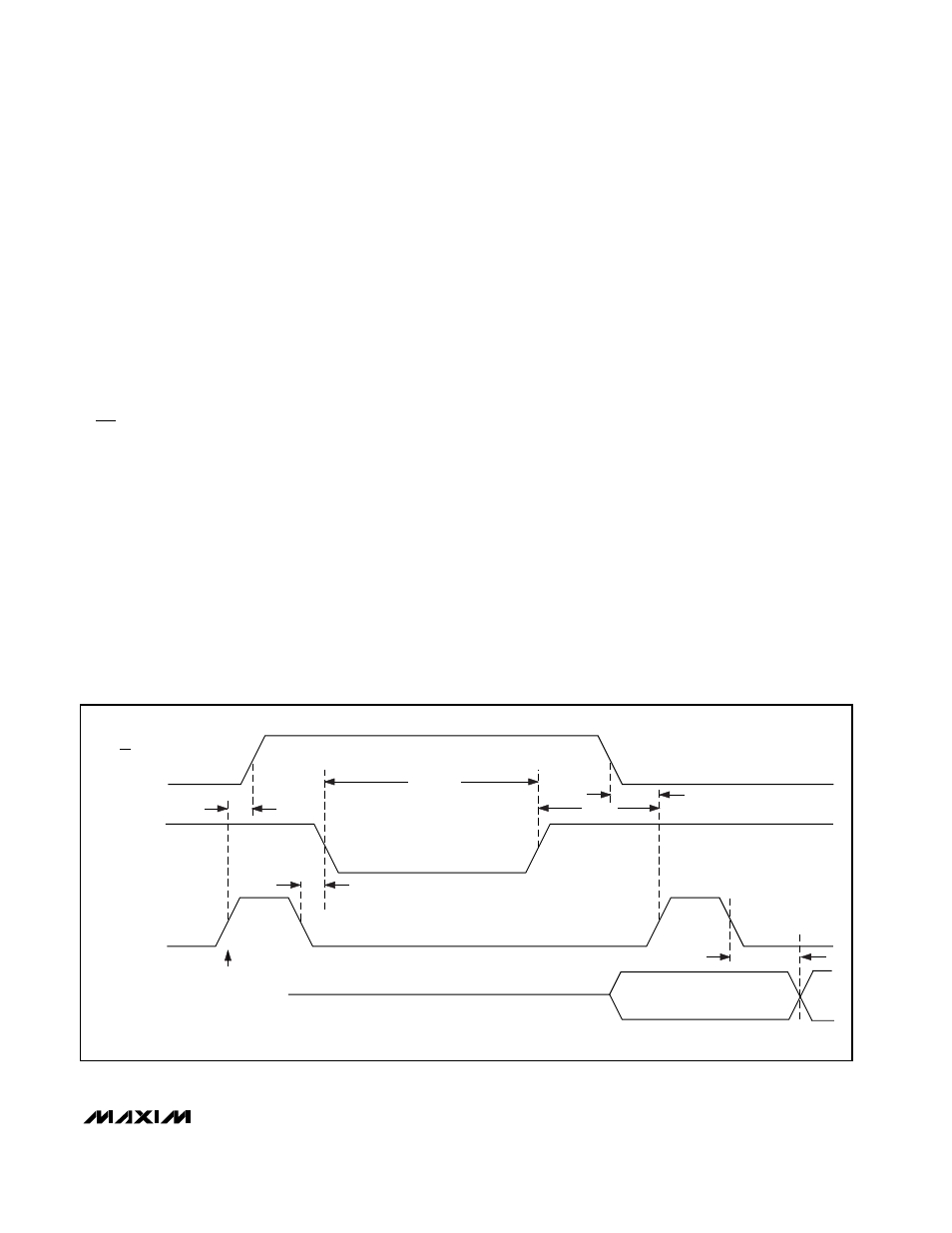
Data Framing
The falling edge of CS does
not
start a conversion. The
first logic high clocked into DIN is interpreted as a start
bit and defines the first bit of the control byte. A conver-
sion starts on the falling edge of SCLK, after the eighth
bit of the control byte (the PD0 bit) is clocked into DIN.
The start bit is defined as:
The first high bit clocked into DIN with CS low any
time the converter is idle; e.g., after V
DD
is applied.
OR
The first high bit clocked into DIN after bit 3 of a con-
version in progress is clocked onto the DOUT pin.
If CS is toggled before the current conversion is com-
plete, the next high bit clocked into DIN is recognized as
a start bit; the current conversion is terminated, and a
new one is started.
The fastest the MAX1248/MAX1249 can run with CS
held low between conversions is 15 clocks per conver-
sion. Figure 10a shows the serial-interface timing nec-
essary to perform a conversion every 15 SCLK cycles
in external clock mode. If CS is tied low and SCLK is
continuous, guarantee a start bit by first clocking in 16
zeros.
Most microcontrollers require that conversions occur in
multiples of 8 SCLK clocks; 16 clocks per conversion is
typically the fastest that a microcontroller can drive the
MAX1248/MAX1249. Figure 10b shows the serial-inter-
face timing necessary to perform a conversion every 16
SCLK cycles in external clock mode.
__________ Applications Information
Power-On Reset
When power is first applied, and if SHDN is not pulled
low, internal power-on reset circuitry activates the
MAX1248/MAX1249 in internal clock mode, ready to
convert with SSTRB = high. After the power supplies
have stabilized, the internal reset time is 10µs, and no
conversions should be performed during this phase.
SSTRB is high on power-up and, if CS is low, the first
logical 1 on DIN is interpreted as a start bit. Until a con-
version takes place, DOUT shifts out zeros (also see
Table 4).
Reference-Buffer Compensation
In addition to its shutdown function, SHDN selects inter-
nal or external compensation. The compensation
affects both power-up time and maximum conversion
speed. The 100kHz minimum clock rate is limited by
droop on the sample-and-hold, and is independent of
the compensation used.
PD0 CLOCK IN
t
SSTRB
t
CSH
t
CONV
t
SCK
SSTRB
SCLK
DOUT
t
CSS
t
DO
NOTE: FOR BEST NOISE PERFORMANCE, KEEP SCLK LOW DURING CONVERSION.
CS
• • •
• • •
• • •
• • •
Figure 9. Internal Clock Mode SSTRB Detailed Timing