Detailed description, Pseudo-differential input, Track/hold – Rainbow Electronics MAX1113 User Manual
Page 8
MAX1112/MAX1113
+5V, Low-Power, Multi-Channel,
Serial 8-Bit ADCs
8
_______________________________________________________________________________________
_______________Detailed Description
The MAX1112/MAX1113 analog-to-digital converters
(ADCs) use a successive-approximation conversion
technique and input track/hold (T/H) circuitry to convert
an analog signal to an 8-bit digital output. A flexible seri-
al interface provides easy interface to microprocessors
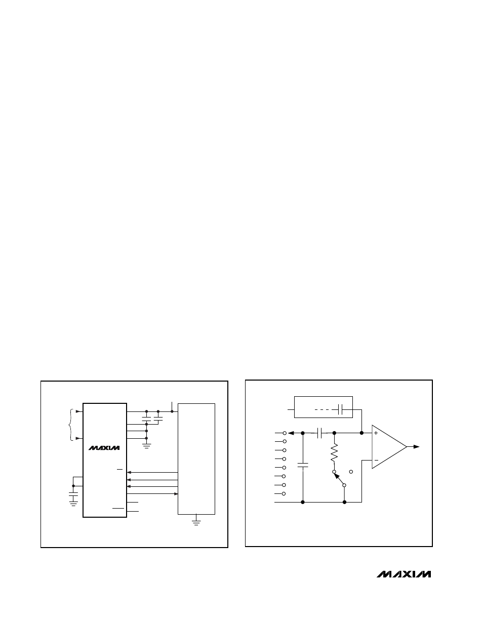
(µPs). Figure 3 shows the Typical Operating Circuit.
Pseudo-Differential Input
The sampling architecture of the ADC’s analog com-
parator is illustrated in Figure 4, the equivalent input cir-
cuit. In single-ended mode, IN+ is internally switched to
the selected input channel, CH_, and IN- is switched to
COM. In differential mode, IN+ and IN- are selected
from the following pairs: CH0/CH1, CH2/CH3,
CH4/CH5, and CH6/CH7. Configure the MAX1112
channels with Table 1 and the MAX1113 channels with
Table 2.
In differential mode, IN- and IN+ are internally switched
to either of the analog inputs. This configuration is
pseudo-differential to the effect that only the signal at
IN+ is sampled. The return side (IN-) must remain sta-
ble within ±0.5LSB (±0.1LSB for best results) with
respect to AGND during a conversion. To accomplish
this, connect a 0.1µF capacitor from IN- (the selected
analog input) to AGND if necessary.
During the acquisition interval, the channel selected as
the positive input (IN+) charges capacitor C
HOLD
. The
acquisition interval spans two SCLK cycles and ends
on the falling SCLK edge after the last bit of the input
control word has been entered. At the end of the acqui-
sition interval, the T/H switch opens, retaining charge
on C
HOLD
as a sample of the signal at IN+.
The conversion interval begins with the input multiplex-
er switching C
HOLD
from the positive input (IN+) to the
negative input (IN-). In single-ended mode, IN- is sim-
ply COM. This unbalances node ZERO at the input of
the comparator. The capacitive DAC adjusts during the
remainder of the conversion cycle to restore node
ZERO to 0V within the limits of 8-bit resolution. This
action is equivalent to transferring a charge of 18pF x
(V
IN+
- V
IN-
) from C
HOLD
to the binary-weighted capac-
itive DAC, which in turn forms a digital representation of
the analog input signal.
Track/Hold
The T/H enters its tracking mode on the falling clock
edge after the sixth bit of the 8-bit control byte has
been shifted in. It enters its hold mode on the falling
clock edge after the eighth bit of the control byte has
been shifted in. If the converter is set up for single-
ended inputs, IN- is connected to COM, and the con-
verter samples the “+” input; if it is set up for differential
inputs, IN- connects to the “-” input, and the difference
(IN+ - IN-) is sampled. At the end of the conversion, the
positive input connects back to IN+, and C
HOLD
charges to the input signal.
V
DD
I/O
SCK (SK)
MOSI (SO)
MISO (SI)
V
SS
SHDN
SSTRB
DOUT
DIN
SCLK
CS
COM
DGND
AGND
V
DD
CH7
1
µ
F
0.1
µ
F
1
µ
F
CH0
ANALOG
INPUTS
MAX1112
MAX1113
CPU
+5V
REFIN
REFOUT
Figure 3. Typical Operating Circuit
CH0
CH1
CH2
CH3
CH4*
CH5*
CH6*
CH7*
COM
C
SWITCH
TRACK
T/H
SWITCH
C
HOLD
HOLD
CAPACITIVE DAC
REFIN
ZERO
COMPARATOR
–
+
18pF
6.5k
R
IN
SINGLE-ENDED MODE: IN+ = CHO–CH7, IN- = COM.
DIFFERENTIAL MODE: IN+ AND IN- SELECTED FROM PAIRS OF
CH0/CH1, CH2/CH3, CH4*/CH5*, CH6*/CH7*.
*MAX1112 ONLY
AT THE SAMPLING INSTANT,
THE MUX INPUT SWITCHES
FROM THE SELECTED IN+
CHANNEL TO THE SELECTED
IN- CHANNEL.
INPUT
MUX
Figure 4. Equivalent Input Circuit