Electrical characteristics (continued) – Rainbow Electronics MAX1113 User Manual
Page 3
µA
MAX1112/MAX1113
+5V, Low-Power, Multi-Channel,
Serial 8-Bit ADCs
_______________________________________________________________________________________
3
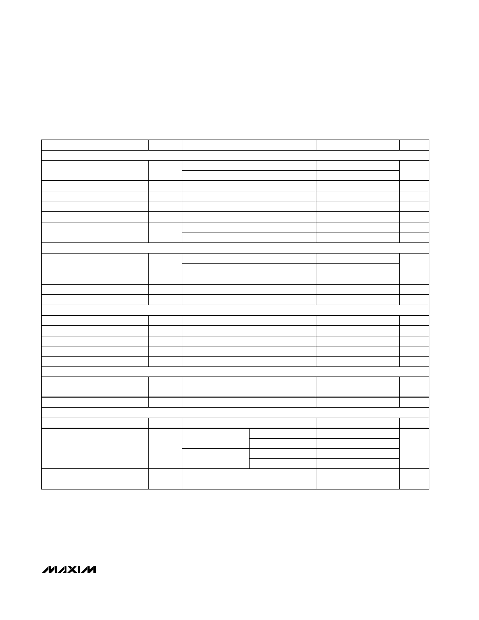
ELECTRICAL CHARACTERISTICS (continued)
(V
DD
= +4.5V to +5.5V; unipolar input mode; COM = 0V; f
SCLK
= 500kHz, external clock (50% duty cycle); 10 clocks/conversion
cycle (50ksps); 1µF capacitor at REFOUT; T
A
= T
MIN
to T
MAX
; unless otherwise noted.)
On/off leakage current, V
CH_
= 0V or V
DD
Used for data transfer only
(Note 5)
External clock, 2MHz
CONDITIONS
ppm/°C
±50
mA
6
REFOUT Short-Circuit Current
pF
18
Input Capacitance
µA
±0.01
±1
Multiplexer Leakage Current
1
2
50
500
kHz
400
Internal Clock Frequency
0mA to 0.5mA output load
mV
4.5
Load Regulation (Note 7)
ns
10
Aperture Delay
µs
1
t
ACQ
Track/Hold Acquisition Time
UNITS
MIN
TYP
MAX
SYMBOL
PARAMETER
ps
V
1
V
DD
+
50mV
Input Voltage Range
(Note 8)
µA
1
20
Input Current
<50
Aperture Jitter
External clock, 500kHz, 10 clocks/conversion
20
Internal clock
µs
25
55
t
CONV
Conversion Time (Note 4)
Bipolar input, COM = V
REFIN
/ 2
Unipolar input, COM = 0V
COM ±
V
REFIN
/ 2
V
0
V
REFIN
Input Voltage Range, Single-
Ended and Differential (Note 6)
V
3.936
4.096
4.256
REFOUT Voltage
External Clock-Frequency Range
MHz
kHz
Capacitive Bypass at REFOUT
µF
REFOUT Temperature Coefficient
V
4.5
5.5
V
DD
Supply Voltage
V
DD
= 4.5V to 5.5V; external reference,
4.096V; full-scale input
mV
±0.4
±4
PSR
Power-Supply Rejection
(Note 9)
2
Power-down
3.2
10
Software
SHDN at DGND
Operating mode
135
250
Full-scale input
C
LOAD
= 10pF
Reference disabled
95
I
DD
µA
Supply Current
CONVERSION RATE
ANALOG INPUT
INTERNAL REFERENCE
EXTERNAL REFERENCE AT REFIN
POWER REQUIREMENTS