Clock modes – Rainbow Electronics MAX1113 User Manual
Page 13

MAX1112/MAX1113
+5V, Low-Power, Multi-Channel,
Serial 8-Bit ADCs
______________________________________________________________________________________
13
Digital Output
In unipolar input mode, the output is straight binary
(Figure 15). For bipolar inputs, the output is two’s-com-
plement (Figure 16). Data is clocked out at SCLK’s
falling edge in MSB-first format.
Clock Modes
The MAX1112/MAX1113 can use either an external ser-
ial clock or the internal clock to perform the successive-
approximation conversion. In both clock modes, the
external clock shifts data in and out of the devices. Bit
PD0 of the control byte programs the clock mode.
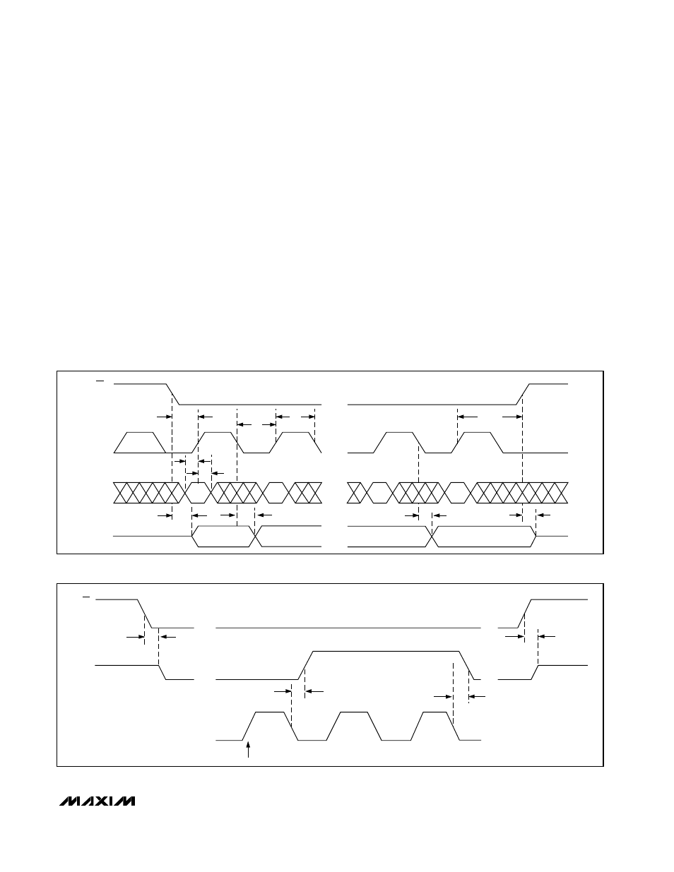
Figures 8–11 show the timing characteristics common
to both modes.
External Clock
In external clock mode, the external clock not only
shifts data in and out, it also drives the analog-to-digital
conversion steps. SSTRB pulses high for two clock
periods after the last bit of the control byte. Successive-
approximation bit decisions are made and appear at
DOUT on each of the next eight SCLK falling edges
(Figure 7). After the eight data bits are clocked out,
subsequent clock pulses clock out zeros from the
DOUT pin.
SSTRB and DOUT go into a high-impedance state
when CS goes high; after the next CS falling edge,
SSTRB outputs a logic low. Figure 9 shows the SSTRB
timing in external clock mode.
The conversion must complete in 1ms, or droop on the
sample-and-hold capacitors may degrade conversion
results. Use internal clock mode if the serial-clock fre-
quency is less than 50kHz, or if serial-clock interruptions
could cause the conversion interval to exceed 1ms.
• • •
• • •
• • •
• • •
CS
SCLK
DIN
DOUT
t
CSS
t
CL
t
DS
t
DH
t
DV
t
DO
t
CH
t
DO
t
TR
t
CSH
Figure 8. Detailed Serial-Interface Timing
• • •
• • •
• • •
• • • •
• • •
t
SDV
t
SSTRB
PD0 CLOCKED IN
t
STR
SSTRB
SCLK
CS
t
SSTRB
• • • •
Figure 9. External Clock Mode SSTRB Detailed Timing
