Rainbow Electronics MAX1113 User Manual
Page 15
MAX1112/MAX1113
+5V, Low-Power, Multi-Channel,
Serial 8-Bit ADCs
______________________________________________________________________________________
15
SCLK
DIN
DOUT
CS
S
CONTROL BYTE 0
CONTROL BYTE 1
S
CONVERSION RESULT 0
B7 B0
B7 B0
B7
CONVERSION RESULT 1
CONVERSION RESULT 2
SSTRB
CONTROL BYTE 2
S
1
8
8
8
10
1
10
1
10
1
CONTROL BYTE 3
S
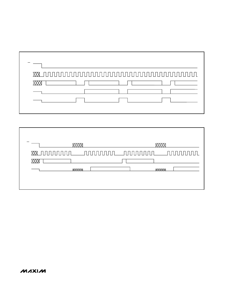
Figure 12a. Continuous Conversions, External Clock Mode, 10 Clocks/Conversion Timing
CS
SCLK
DIN
DOUT
S
CONTROL BYTE 0
CONTROL BYTE 1
S
CONVERSION RESULT 0
B7 B0
B7
CONVERSION RESULT 1
Figure 12b. Continuous Conversions, External Clock Mode, 16 Clocks/Conversion Timing
Data Framing
The falling edge of CS does not start a conversion. The
first logic high clocked into DIN is interpreted as a start
bit and defines the first bit of the control byte. A conver-
sion starts on the falling edge of SCLK, after the eighth
bit of the control byte (the PD0 bit) is clocked into DIN.
The start bit is defined as:
The first high bit clocked into DIN with CS low any
time the converter is idle, e.g., after V
DD
is applied.
OR
The first high bit clocked into DIN after the MSB of a
conversion in progress is clocked onto the DOUT
pin.
If CS is toggled before the current conversion is com-
plete, then the next high bit clocked into DIN is recog-
nized as a start bit; the current conversion is
terminated, and a new one is started.
The fastest the MAX1112/MAX1113 can run is 10
clocks per conversion. Figure 12a shows the serial-
interface timing necessary to perform a conversion
every 10 SCLK cycles in external clock mode.
Many microcontrollers require that conversions occur in
multiples of eight SCLK clocks; 16 clocks per conver-
sion is typically the fastest that a microcontroller can
drive the MAX1112/MAX1113. Figure 12b shows the
serial-interface timing necessary to perform a conver-
sion every 16 SCLK cycles in external clock mode.