Detailed description – Rainbow Electronics MAX1093 User Manual
Page 9
Detailed Description
Converter Operation
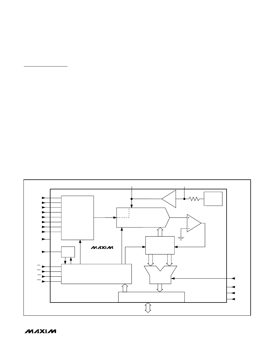
The MAX1091/MAX1093 ADCs use a successive-
approximation (SAR) conversion technique and an
input track/hold (T/H) stage to convert an analog input
signal to a 10-bit digital output. Their parallel 8+2 out-
put format provides an easy interface to standard
microprocessors (µPs). Figure 2 shows the simplified
internal architecture of the MAX1091/MAX1093.
Single-Ended and
Pseudo-Differential Operation
The sampling architecture of the ADC’s analog com-
parator is illustrated in the equivalent input circuit in
Figure 3. In single-ended mode, IN+ is internally
switched to channels CH0–CH7 for the MAX1091
(Figure 3a) and to CH0–CH3 for the MAX1093 (Figure
3b), while IN- is switched to COM (Table 3).
In differential mode IN+ and IN- are selected from ana-
log input pairs (Table 4) and are internally switched to
either of the analog inputs. This configuration is pseu-
do-differential in that only the signal at IN+ is sampled.
The return side (IN-) must remain stable within ±0.5LSB
(±0.1LSB for best performance) with respect to GND
during a conversion. To accomplish this, connect a
0.1µF capacitor from IN- (the selected input) to GND.
During the acquisition interval, the channel selected as
the positive input (IN+) charges capacitor C
HOLD
. At
the end of the acquisition interval, the T/H switch
opens, retaining charge on C
HOLD
as a sample of the
signal at IN+.
The conversion interval begins with the input multiplex-
er switching C
HOLD
from the positive input (IN+) to the
negative input (IN-). This unbalances node ZERO at the
comparator’s positive input. The capacitive digital-to-
analog converter (DAC) adjusts during the remainder of
the conversion cycle to restore node ZERO to 0V within
the limits of 10-bit resolution. This action is equivalent to
transferring a 12pF[(V
IN+
) - (V
IN-
)] charge from C
HOLD
to the binary-weighted capacitive DAC, which in turn
forms a digital representation of the analog input signal.
MAX1091/MAX1093
250ksps, +3V, 8-/4-Channel, 10-Bit ADCs
with +2.5V Reference and Parallel Interface
_______________________________________________________________________________________
9
T/H
THREE-STATE, BIDIRECTIONAL
I/O INTERFACE
10
17k
8
8
2
8
2
8
SUCCESSIVE-
APPROXIMATION
REGISTER
MUX
CHARGE REDISTRIBUTION
10-BIT DAC
CLOCK
( ) ARE FOR MAX1091 ONLY.
ANALOG
INPUT
MULTIPLEXER
CONTROL LOGIC
&
LATCHES
REF
REFADJ
1.22V
REFERENCE
D0–D7
8-BIT DATA BUS
(CH5)
(CH4)
(CH7)
(CH6)
CH3
CH2
CH1
CH0
COM
CLK
CS
WR
RD
V
DD
HBEN
GND
V
LOGIC
MAX1091
MAX1093
A
V
=
2.05
COMP
INT
Figure 2. Simplified Internal Architecture for 8-/4-Channel MAX1091/MAX1093