Rainbow Electronics MAX1093 User Manual
Page 16
MAX1091/MAX1093
When applying an external reference to REF, disable
the internal reference buffer by connecting REFADJ to
V
DD
. The DC input resistance at REF is 25k
Ω.
Therefore, an external reference at REF must deliver up
to 200µA DC load current during a conversion and
have an output impedance less than 10
Ω. If the refer-
ence has higher output impedance or is noisy, bypass
it close to the REF pin with a 4.7µF capacitor.
Power-Down Modes
Save power by placing the converter in a low-current
shutdown state between conversions. Select standby
mode or shutdown mode via bits D6 and D7 of the con-
trol byte (Tables 1 and 2). In both software power-down
modes, the parallel interface remains active, but the
ADC does not convert.
Standby Mode
While in standby mode, the supply current is 850µA
(typ). The part will power up on the next rising edge on
WR and is ready to perform conversions. This quick
turn-on time allows the user to realize significantly
reduced power consumption for conversion rates
below 250ksps.
Shutdown Mode
Shutdown mode turns off all chip functions that draw qui-
escent current, reducing the typical supply current to
2µA immediately after the current conversion is complet-
ed. A rising edge on WR causes the MAX1091/MAX1093
to exit shutdown mode and return to normal operation.
To achieve full 10-bit accuracy with a 4.7µF reference
bypass capacitor, 500µs is required after power-up.
Waiting this 500µs in standby mode instead of in full-
power mode can reduce power consumption by a factor
of 3 or more. When using an external reference, only
50µs is required after power-up. Enter standby mode by
performing a dummy conversion with the control byte
specifying standby mode.
Note: Bypassing capacitors larger than 4.7µF between
REF and GND will result in longer power-up delays.
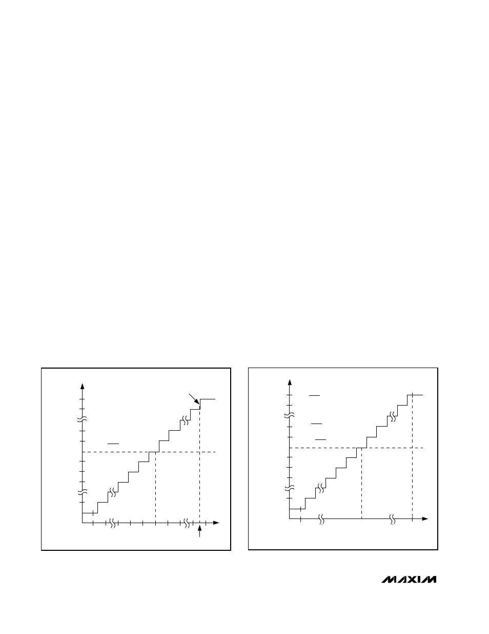
Transfer Function
Table 6 shows the full-scale voltage ranges for unipolar
and bipolar modes.
Figure 8 depicts the nominal, unipolar input/output (I/O)
transfer function and Figure 9 shows the bipolar I/O
transfer function. Code transitions occur halfway
between successive-integer LSB values. Output coding
is binary, with 1LSB = V
REF
/ 1024.
Maximum Sampling Rate/
Achieving 300ksps
When running at the maximum clock frequency of
4.8MHz, the specified throughput of 250ksps is
achieved by completing a conversion every 19 clock
cycles: 1 write cycle, 3 acquisition cycles, 13 conver-
250ksps, +3V, 8-/4-Channel, 10-Bit ADCs
with +2.5V Reference and Parallel Interface
16
______________________________________________________________________________________
111 . . . 111
111 . . . 110
100 . . . 010
100 . . . 001
100 . . . 000
011 . . . 111
011 . . . 110
011 . . . 101
000 . . . 001
000 . . . 000
1
0
2
INPUT VOLTAGE (LSB)
OUTPUT CODE
ZS = COM
FS = REF + COM
FS
512
(COM)
1LSB =
REF
1024
FS -
3
/
2
LSB
FULL-SCALE
TRANSITION
Figure 8. Unipolar Transfer Function
011 . . . 111
011 . . . 110
000 . . . 010
000 . . . 001
000 . . . 000
111 . . . 111
111 . . . 110
111 . . . 101
100 . . . 001
100 . . . 000
- FS
COM*
INPUT VOLTAGE (LSB)
OUTPUT CODE
ZS = COM
+FS - 1LSB
*COM
≥ V
REF
/2
+ COM
FS
=
REF
2
-FS =
+ COM
-REF
2
1LSB =
REF
1024
Figure 9. Bipolar Transfer Function