Rainbow Electronics MAX1093 User Manual
Page 10
MAX1091/MAX1093
Analog Input Protection
Internal protection diodes, which clamp the analog
input to V
DD
and GND, allow each input channel to
swing within (GND - 300mV) to (V
DD
+ 300mV) without
damage. However, for accurate conversions near full
scale, both inputs must not exceed (V
DD
+ 50mV) or be
less than (GND - 50mV).
If an off-channel analog input voltage exceeds the
supplies by more than 50mV, limit the forward-bias
input current to 4mA.
Track/Hold
The MAX1091/MAX1093 T/H stage enters its tracking
mode on the rising edge of WR. In external acquisition
mode, the part enters its hold mode on the next rising
edge of WR. In internal acquisition mode, the part
enters its hold mode on the fourth falling edge of clock
after writing the control byte. Note that in internal clock
mode this occurs approximately 1µs after writing the
control byte. In single-ended operation, IN- is connect-
ed to COM and the converter samples the positive (+)
input. In pseudo-differential operation, IN- connects to
the negative input (-), and the difference of
(IN+) - (IN-) is
sampled. At the beginning of the next conversion, the
positive input connects back to IN+ and C
HOLD
charges to the input signal.
The time required for the T/H stage to acquire an input
signal depends on how quickly its input capacitance is
charged. If the input signal’s source impedance is high,
the acquisition time lengthens, and more time must be
allowed between conversions. The acquisition time,
t
ACQ
, is the maximum time the device takes to acquire
the signal and is also the minimum time required for the
signal to be acquired. Calculate this with the following
equation:
t
ACQ
= 7 (R
S
+ R
IN
) C
IN
where R
S
is the source impedance of the input signal,
R
IN
(800
Ω) is the input resistance, and C
IN
(12pF) is
the ADC’s input capacitance. Source impedances
below 3k
Ω have no significant impact on the MAX1091/
MAX1093’s AC performance.
Higher source impedances can be used if a 0.01µF
capacitor is connected to the individual analog inputs.
Together with the input impedance, this capacitor
forms an RC filter, limiting the ADC’s signal bandwidth.
Input Bandwidth
The MAX1091/MAX1093 T/H stage offers a 250kHz full-
linear and a 3MHz full-power bandwidth, enabling
these parts to use undersampling techniques to digitize
high-speed transients and measure periodic signals
with bandwidths exceeding the ADCs sampling rate. To
avoid high-frequency signals being aliased into the fre-
quency band of interest, anti-alias filtering is recom-
mended.
Starting a Conversion
Initiate a conversion by writing a control byte that
selects the multiplexer channel and configures the
MAX1091/MAX1093 for either unipolar or bipolar opera-
tion. A write pulse (WR + CS) can either start an acqui-
sition interval or initiate a combined acquisition plus
250ksps, +3V, 8-/4-Channel, 10-Bit ADCs
with +2.5V Reference and Parallel Interface
10
______________________________________________________________________________________
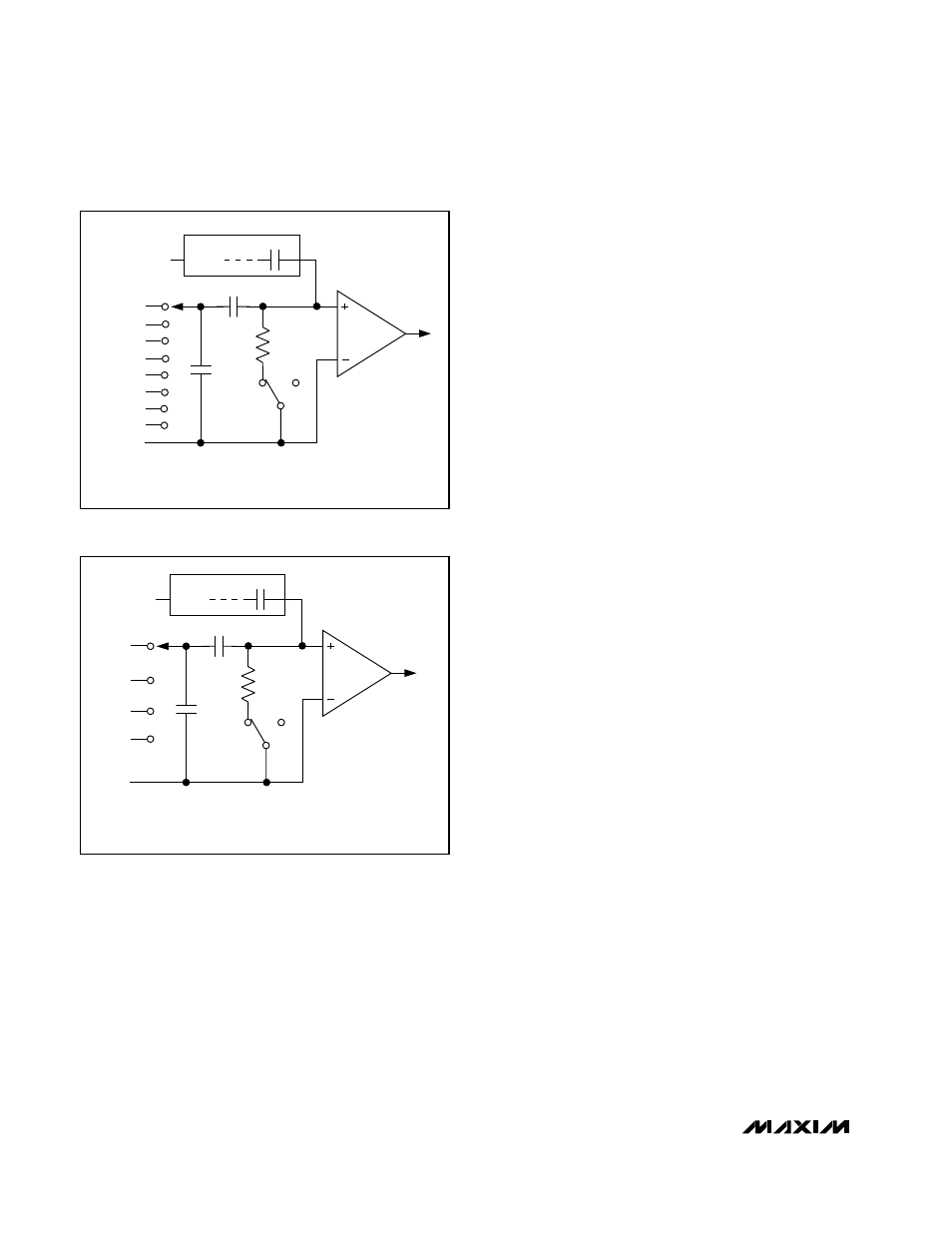
CH0
CH2
CH1
CH3
CH4
CH6
CH7
CH5
COM
C
SWITCH
TRACK
T/H
SWITCH
R
IN
800
Ω
C
HOLD
HOLD
10-BIT CAPACITIVE DAC
REF
ZERO
COMPARATOR
–
+
12pF
SINGLE-ENDED MODE: IN+ = CH0–CH7, IN- = COM
PSEUDO-DIFFERENTIAL MODE: IN+ AND IN- SELECTED FROM PAIRS OF
CH0/CH1, CH2/CH3, CH4/CH5, AND CH6/CH7
AT THE SAMPLING INSTANT,
THE MUX INPUT SWITCHES
FROM THE SELECTED IN+
CHANNEL TO THE SELECTED
IN- CHANNEL.
INPUT
MUX
Figure 3a. MAX1091 Simplified Input Structure
CH0
CH1
CH2
CH3
COM
C
SWITCH
TRACK
T/H
SWITCH
R
IN
800
Ω
C
HOLD
HOLD
10-BIT CAPACITIVE DAC
REF
ZERO
COMPARATOR
–
+
12pF
SINGLE-ENDED MODE: IN+ = CH0–CH3, IN- = COM
PSEUDO-DIFFERENTIAL MODE: IN+ AND IN- SELECTED FROM PAIRS OF
CH0/CH1 AND CH2/CH3
AT THE SAMPLING INSTANT,
THE MUX INPUT SWITCHES
FROM THE SELECTED IN+
CHANNEL TO THE SELECTED
IN- CHANNEL.
INPUT
MUX
Figure 3b. MAX1093 Simplified Input Structure