Where r, Is the analog input source impedance, r, 5k ω, and c – Rainbow Electronics MAX1039 User Manual
Page 9: 18pf. t, Is 1/f, Allow 625ns for t

of the address byte (see the Slave Address section).
The T/H circuitry enters hold mode two internal clock
cycles later. A conversion or series of conversions are
then internally clocked (eight clock cycles per conver-
sion) and the MAX1036–MAX1039 hold SCL low. When
operating in external clock mode, the T/H circuitry
enters track mode on the seventh falling edge of a valid
slave address byte. Hold mode is then entered on the
falling edge of the eighth clock cycle. The conversion is
performed during the next eight clock cycles.
The time required for the T/H circuitry to acquire an
input signal is a function of input capacitance. If the
analog input source impedance is high, the acquisition
time lengthens and more time must be allowed
between conversions. The acquisition time (t
ACQ
) is the
minimum time needed for the signal to be acquired. It
is calculated by:
t
ACQ
≥ 6.25
✕
(R
SOURCE
+ R
IN
)
✕
C
IN
where R
SOURCE
is the analog input source impedance,
R
IN
= 2.5k
Ω, and C
IN
= 18pF. t
ACQ
is 1/f
SCL
for external
clock mode. For internal clock mode, the acquisition
time is two internal clock cycles. To select R
SOURCE
,
allow 625ns for t
ACQ
in internal clock mode to account
for clock frequency variations.
MAX1036–MAX1039
2.7V to 5.5V, Low-Power, 4-/12-Channel
2-Wire Serial 8-Bit ADCs
_______________________________________________________________________________________
9
t
HD.STA
t
SU.DAT
t
HIGH
t
R
t
F
t
HD.DAT
t
HD.STA
S
Sr
A
SCL
SDA
t
SU.STA
t
LOW
t
BUF
t
SU.STO
P
S
t
HD.STA
t
SU.DAT
t
HIGH
t
FCL
t
HD.DAT
t
HD.STA
S
Sr
A
SCL
SDA
t
SU.STA
t
LOW
t
BUF
t
SU.STO
S
t
RCL
t
RCL1
HS-MODE
F/S-MODE
A. F/S-MODE I
2
C SERIAL INTERFACE TIMING
B. HS-MODE I
2
C SERIAL INTERFACE TIMING
t
FDA
t
RDA
t
t
R
t
F
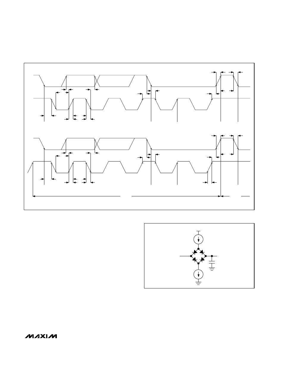
Figure 1. I
2
C Serial Interface Timing
V
DD
I
OL
= 3mA
I
OH
= 0mA
V
OUT
400pF
SDA
Figure 2. Load Circuit
