Rainbow Electronics MAX1039 User Manual
Page 2
MAX1036–MAX1039
2.7V to 5.5V, Low-Power, 4-/12-Channel
2-Wire Serial 8-Bit ADCs
2
_______________________________________________________________________________________
ABSOLUTE MAXIMUM RATINGS
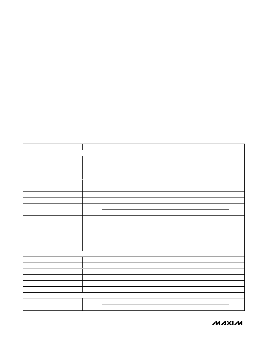
ELECTRICAL CHARACTERISTICS
(V
DD
= 2.7V to 3.6V (MAX1037/MAX1039), V
DD
= 4.5V to 5.5V (MAX1036/MAX1038). External reference, V
REF
= 2.048V
(MAX1037/MAX1039), V
REF
= 4.096V (MAX1036/MAX1038). External clock, f
SCL
= 1.7MHz, T
A
= T
MIN
to T
MAX
, unless otherwise
noted. Typical values are at T
A
= +25°C.)
Stresses beyond those listed under “Absolute Maximum Ratings” may cause permanent damage to the device. These are stress ratings only, and functional
operation of the device at these or any other conditions beyond those indicated in the operational sections of the specifications is not implied. Exposure to
absolute maximum rating conditions for extended periods may affect device reliability.
V
DD
to GND ..............................................................-0.3V to +6V
AIN0–AIN11, REF to
GND ......................-0.3V to the lower of (V
DD
+ 0.3V) and +6V
SDA, SCL to GND.....................................................-0.3V to +6V
Maximum Current Into Any Pin .........................................±50mA
Continuous Power Dissipation (T
A
= +70°C)
8-Pin SOT23 (derate 7.1mW/°C above +70°C).............567mW
16-Pin QSOP (derate 8.3mW/°C above +70°C).........666.7mW
Operating Temperature Range ...........................-40°C to +85°C
Junction Temperature ......................................................+150°C
Storage Temperature Range .............................-60°C to +150°C
Lead Temperature (soldering, 10s) .................................+300°C
PARAMETER
SYMBOL
CONDITIONS
MIN
TYP
MAX
UNITS
DC ACCURACY (Note 1)
Resolution
8
Bits
Relative Accuracy
INL
(Note 2)
±1
LSB
Differential Nonlinearity
DNL
No missing codes over temperature
±1
LSB
Offset Error
±1.5
LSB
Offset Error Temperature
Coefficient
3
ppm/
°C
Gain Error
(Note 3)
±1
LSB
Gain Temperature Coefficient
±1
ppm/
°C
MAX1036/MAX1037
±0.5
±2
Total Unadjusted Error
TUE
MAX1038A/MAX1039A
±0.5
±1
LSB
Channel-to-Channel Offset
Matching
±0.1
LSB
Channel-to-Channel Gain
Matching
±0.5
LSB
Input Common-Mode Rejection
Ratio
CMRR
Pseudo-differential input mode
75
dB
DYNAMIC PERFORMANCE (f
IN(sine wave)
= 25kHz, V
IN
= V
REF(P-P)
, f
SAMPLE
= 188ksps, R
IN
= 100
Ω)
Signal-to-Noise Plus Distortion
SINAD
49
dB
Total Harmonic Distortion
THD
Up to the 5th harmonic
-69
dB
Spurious-Free Dynamic Range
SFDR
69
dB
Channel-to-Channel Crosstalk
(Note 4)
75
dB
Full-Power Bandwidth
-3dB point
2.0
MHz
Full-Linear Bandwidth
SINAD > 49dB
200
kHz
CONVERSION RATE
Internal clock
6.1
Conversion Time (Note 5)
t
CONV
External clock
4.7
µs