Pin description – Rainbow Electronics MAX1664 User Manual
Page 7
MAX1664
Active-Matrix Liquid Crystal Display
(AMLCD) Supply
_______________________________________________________________________________________
7
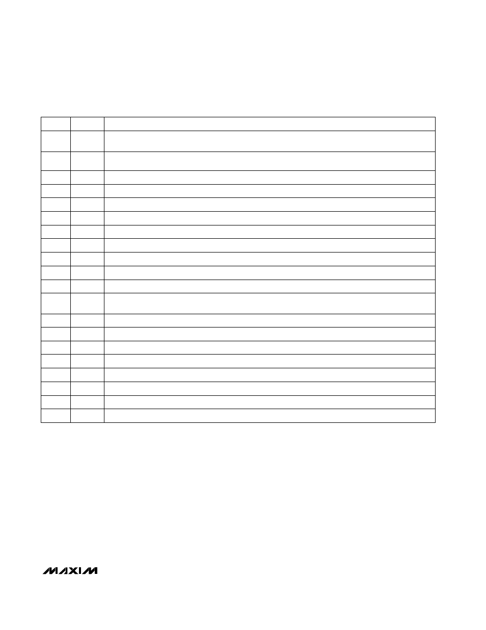
PLL Compensation. Connect compensation network as in Figure 4.
PLLC
9
Backplane Driver Negative Supply. Typically connected to PGND1. May be connected to a separate supply.
BPV
SS
10
Backplane Driver Output
BPDRV
11
Backplane Driver Positive Supply. Typically connected to V
OUT1
of DC-DC 1. May be connected to a
separate supply.
BPV
DD
12
Backplane Driver Clock Input. See Table 1 for input frequency ranges.
BPCLK
13
Analog Ground. Connect to PGND1 and PGND2. See
Supply Connections and Layout
section.
GND
5
Supply Input to the IC. The input voltage range is +2.8V to +5.5V.
IN
6
Regulator Feedback Input for Negative Output, DC-DC 2. Regulates to 0V nominal.
FB2-
7
Regulator Feedback Input for Positive Output, DC-DC 2. Regulates to 1.25V nominal.
FB2+
8
Internal Reference Output. Connect a 0.22µF capacitor from this pin to GND. REF can source up to 50µA.
REF
4
Regulator Feedback Input, DC-DC 1. Regulates to 1.25V nominal.
FB1
3
PIN
Ready Indicator Output, DC-DC 1 and DC-DC 2. Open-drain N-channel output becomes high impedance
when all three outputs are within 10% of regulation.
RDY
2
Shutdown Input. Drive low to enter shutdown mode. Drive high or connect to IN for normal operation. All IC
sections are off when SHDN is low.
SHDN
1
FUNCTION
NAME
Power Ground 1. Connect to PGND2. Source of internal LX1 N-channel MOSFET.
PGND1
18
Drain of Internal LX1 N-Channel MOSFET
LX1
19
Sets the BPCLK input frequency range for PLL synchronization. Connect to GND, REF, or IN. See Table 1.
FPLL
20
DC-DC 2 Power Input. Source of Internal LX2P P-channel MOSFET.
INP
14
Drain of Internal LX2P P-Channel MOSFET
LX2P
15
Drain of Internal LX2N N-Channel MOSFET
LX2N
16
Power Ground 2. Connect to PGND1. Source of internal LX2N N-channel MOSFET.
PGND2
17
______________________________________________________________Pin Description