Inductor selection – Rainbow Electronics MAX1664 User Manual
Page 11
MAX1664
Active-Matrix Liquid Crystal Display
(AMLCD) Supply
______________________________________________________________________________________
11
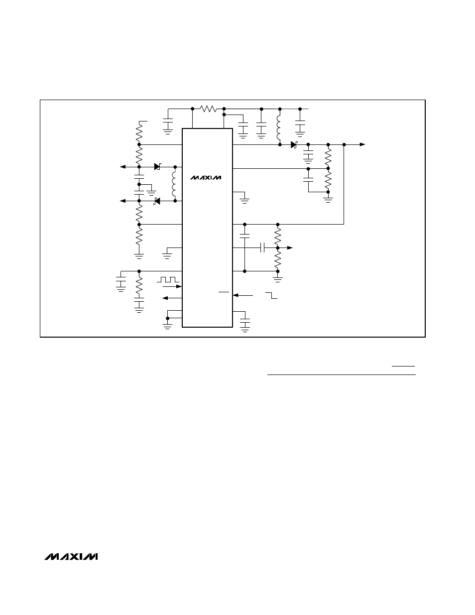
Inductor Selection
The optimum inductor value for L1 is 3.3µH, as shown
in Figure 4. Inductors with less than 300m
Ω
DC series
resistance are recommended to achieve the highest
efficiency. Using a larger value for L1 (e.g., 4.7µH)
increases the output current capability of DC-DC 1 (by
reducing the peak ripple current) at the expense of size
and the additional output filter capacitance needed for
loop stability.
For DC-DC 2, at large input voltages (i.e., 5V) and low
switching frequencies (i.e.,
≤
400kHz), the value of L2
should be increased (e.g., 6.8µH or 10µH) to limit the
peak current. In some cases it may be necessary to
reduce the value of L2 to increase the output current
capability of DC-DC 2 (Table 2). The relationship between
input voltage, output voltage, switching frequency, induc-
tor value, and maximum load current for DC-DC 2 is com-
plex and nonlinear. This relationship is summarized in
Table 2. The L2 equation is as follows:
where:
Internal MOSFET on-resistance:
R
ON(LX2P)
= R
ON(LX2N)
= 0.9
Ω
typical
External inductor DC resistance:
R
L2
= 0.3
Ω
typical
Inductor peak current:
I
PEAK
= 700mA (750mA absolute maximum)
Due to the MAX1664’s high switching frequency, induc-
tors with a high-frequency core material such as ferrite
are recommended. Powdered iron compounds are not
recommended due to their higher core losses. Typical
small-size, low-profile inductors include the ILS-3825
(Dale Electronics-Vishay) and the CLQ61B (Sumida).
These inductors are primarily used for DC-DC
converters with low height requirements. See Table 3
for more information on manufacturers who provide
low-profile inductors.
L2
V
- R
R
R
(I
)
2
I
x 2 f
INP
ON(LX2P)
ON(LX2N)
L2
PEAK
PEAK
DC-DC 1
>
+
+
[
]
(
)
REF
FB2-
IN
INP
LX2P
LX2N
FB2+
R8
49.9k
R7
549k
R6
200k
R5
49.9k
D3
D2
L2
4.7
µ
H
PGND2
PLLC
GND
FPLL
RDY
REF
SHDN
ON
OFF
V
OUT1
5.5V
2.2
µ
F
3 x 10
µ
F
0.22
µ
F
22nF
100k
2.2nF
0.22
µ
F
0.47
µ
F
50pF
2 x 10
µ
F
10
µ
F
10
µ
F
2.2
µ
F
33
Ω
0.47
µ
F
3.3
µ
H
R1
301k
R2
100k
R3
100k
R4
100k
V
OUT2-
-5V
V
OUT2+
15V
BPV
SS
BACKPLANE
DRIVER
V
SUPPLY
2.8V TO 5.5V
BPDRV
BPV
DD
PGND1
FB1
LX1
BPCLK
MAX1664
Figure 4. Detailed Typical Operating Circuit