Applications information, Table 3. component manufacturers – Rainbow Electronics MAX1664 User Manual
Page 13
Ceramic capacitors are recommended because they
have low ESR and the lowest profile. Typical ceramic
capacitors are the C3225X5R series from TDK and
JMK325 series from Taiyo Yuden. See Table 3 for more
information on the manufacturers who provide surface-
mount ceramic capacitors.
PLL Compensation
In most applications, the recommended compensation
component values shown in Figure 4 will give optimal
system performance. If no backplane clock is used,
connect PLLC to REF.
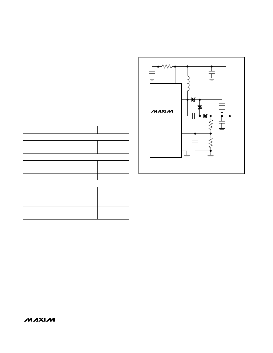
_____________Applications Information
Increasing V
OUT
Above 5.5V
For V
OUT1
output voltages above 5.5V, connect the
supplemental charge pump circuit shown in Figure 5.
The connection shown supplies a 10V 150mA output,
but other voltages from 2 x V
IN
to 10V can be set by
selecting the appropriate values for R1 and R2 (see
DC-DC 1 Output
section). C2–C4 are shown as parallel
combinations of 3.3µF ceramic capacitors so that a
1.1mm height restriction can be met. If height is not
restricted, then larger values can be used instead of
parallel capacitor combinations.
3.3V to -20V Charge-Pump Configuration
For applications requiring negative voltages down to
-20V, an inverting charge-pump block can be added to
the V
OUT2-
output (Figure 6). Typical values for C
F
and
C
OUT
are 0.47µF to 1µF and 4.7µF to 10µF, respective-
ly. As a general rule, C
OUT
should be ten times greater
than C
F
. This circuit operates as follows:
1) During the first PFM cycle, the voltage at V1 is
charged by inductor L2 to some fraction of its final
steady-state voltage, in the normal manner described
in the
Detailed Description
.
2) During the first half of subsequent PFM cycles, pin
LX2P is pulled to V
INP
, and capacitor C
F
is charged
to (V
INP
+
V
1
- V
D
), where V
D
is a diode forward
voltage.
3) During subsequent second half-cycles when LX2P
flies negatively below V1, capacitor C
F
transfers
some of its energy to output capacitor C
OUT
, which
then is charged to a negative voltage of approxi-
mately (V
INP
+ 2 x
V
1
- 2x V
D
).
4) This process continues until V
OUT
reaches the
desired voltage, as determined by the ratio of the
FB2- feedback resistors.
5) During steady-state (in-regulation) operation, the
magnitude of the voltage at LX2P is equal to
(
V
OUT
/ 2 - V
INP
/ 2 + V
D
), which must be limited to
less than 10V.
MAX1664
Active-Matrix Liquid Crystal Display
(AMLCD) Supply
______________________________________________________________________________________
13
MANUFACTURER
PHONE
FAX
Dale Inductors
(605) 668-4131
(605) 665-1627
Sumida USA
(847) 956-0666
(847) 956-0702
Central Semiconductor
(516) 435-1110
(516) 435-1824
International Rectifier
(310) 322-3331
(310) 322-3232
TDK
(847) 390-4373
(847) 390-4428
Vishay/Vitramon
(203) 268-6261
(203) 452-5670
Table 3. Component Manufacturers
MAX1664
LX1
C3
3.3
µ
F (x6)
C4
3.3
µ
F (x2)
R2
13k
D1, D2, D3— MBRM5817
C1, C2, C3—ALL CERAMIC TYPES
R1
91k
C2
3.3
µ
F (x2)
50pF
D2
33
Ω
IN
INP
D3
D1
V
1
10V
150mA
V
SUPPLY
2.8V TO 3.6V
PGND1
FB1
C1
3.3
µ
F (x2)
3.3
µ
H
0.47
µ
F
Figure 5. Charge Pump Configuration to Increase V
OUT1
Above 5.5V.
Motorola
(602) 303-5454
(602) 994-6430
Marcon/United
Chemicon
(847) 696-2000
(847) 696-9278
Taiyo Yuden
(408) 573-4150
(408) 573-4159
INDUCTORS
DIODES
CERAMIC CAPACITORS