Max3983 quad copper-cable signal conditioner, Electrical characteristics (continued) – Rainbow Electronics MAX3983 User Manual
Page 5
MAX3983
Quad Copper-Cable Signal Conditioner
_______________________________________________________________________________________
5
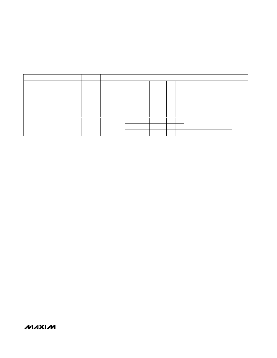
ELECTRICAL CHARACTERISTICS (continued)
(V
CC
= +3.0V to +3.6V, T
A
= 0°C to +85°C. Typical values are at V
CC
= +3.3V and T
A
= +25°C, unless otherwise noted.)
PARAMETER
SYMBOL
CONDITIONS
MIN
TYP
MAX
UNITS
Source to
TX_IN
TX_OUT to RX_IN
TX_PE1
TX_PE0
RX_OUT to Load
RX_PE
1m, 24AWG
0
0
5in
0
15m, 24AWG
1
1
20in
1
0.20
0.25
Residual Output Deterministic
Jitter at 3.2Gbps
(Notes 1, 12, 13, 14)
6-mil FR4
≤
20 in
20m, 24AWG
1
1
20in
1
0.25
0.3
UI
P-P
Note 1:
Guaranteed by design and characterization.
Note 2:
Measured with 2in of FR4 through InfiniBand connector with TX_PE1 = TX_PE0 =1.
Note 3:
Measured at the chip using 0000011111 or equivalent pattern. TX_PE1 = TX_PE0 = 0 for minimum preemphasis.
Note 4:
All channels under test are not transmitting during test. Channel tested with XAUI CJPAT, as well as this pattern: 19 zeros,
1, 10 zeros, 1010101010 (D21.5 character), 1100000101 (K28.5+ character), 19 ones, 0, 10 ones, 0101010101 (D10.2
character), 0011111010 (K28.5- character).
Note 5:
Cables are unequalized, Amphenol Spectra-Strip 24AWG and 28AWG or equivalent equipped with Fujitsu “MicroGiga”
connector or equivalent. All other channels are quiet. Residual deterministic jitter is the difference between the source jit-
ter and the output jitter at the load. The deterministic jitter (DJ) at the output of the transmission line must be from media-
induced loss and not from clock-source modulation. Depending upon the system environment, better results can be
achieved by selecting different preemphasis levels.
Note 6:
Tested with a 1GHz sine wave applied at TX_IN under test with less than 5in of FR4.
Note 7:
Measured with 3in of FR4 with RX_PE = 1.
Note 8:
Measured at the chip using 0000011111 or equivalent pattern. RX_PE = low (minimum). Signal source is 1V
P-P
with 5m,
28AWG InfiniBand cable.
Note 9:
All other receive channels are quiet. TX_ENABLE = 0. Channel tested with XAUI CJPAT as well as this pattern: 19 zeros,
1, 10 zeros, 1010101010 (D21.5 character), 1100000101 (K28.5+ character), 19 ones, 0, 10 ones, 0101010101 (D10.2
character), 0011111010 (K28.5- character).
Note 10: FR4 board material: 6-mil-wide, 100
Ω, edge-coupled stripline (tanδ = 0.022, 4.0 < ε
R
< 4.4).
Note 11: Tested with a 1GHz sine wave applied at RX_IN under test with less than 5in of FR4.
Note 12: Channel tested with XAUI CJPAT as well as this pattern: 19 zeros, 1, 10 zeros, 1010101010 (D21.5 character), 1100000101
(K28.5+ character), 19 ones, 0, 10 ones, 0101010101 (D10.2 character), 0011111010 (K28.5- character).
Note 13: Cables are unequalized, Amphenol Spectra-Strip 24AWG or equivalent equipped with Fujitsu “MicroGiga” connector or
equivalent. Residual deterministic jitter is the difference between the source jitter at point A and the load jitter at point B in
Figure 2. The deterministic jitter (DJ) at the output of the transmission line must be from media-induced loss and not from
clock-source modulation. Depending upon the system environment, better results can be achieved by selecting different
preemphasis levels.
Note 14: Valid with pattern generator deterministic jitter as high as 0.17UI
P-P
.