Max3983 quad copper-cable signal conditioner – Rainbow Electronics MAX3983 User Manual
Page 2
MAX3983
Quad Copper-Cable Signal Conditioner
2
_______________________________________________________________________________________
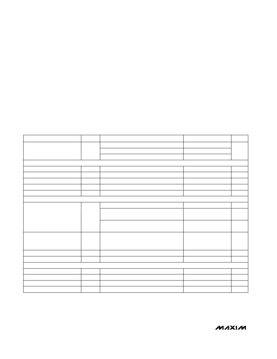
ABSOLUTE MAXIMUM RATINGS
ELECTRICAL CHARACTERISTICS
(V
CC
= +3.0V to +3.6V, T
A
= 0°C to +85°C. Typical values are at V
CC
= +3.3V and T
A
= +25°C, unless otherwise noted.)
Stresses beyond those listed under “Absolute Maximum Ratings” may cause permanent damage to the device. These are stress ratings only, and functional
operation of the device at these or any other conditions beyond those indicated in the operational sections of the specifications is not implied. Exposure to
absolute maximum rating conditions for extended periods may affect device reliability.
Supply Voltage, V
CC
..............................................-0.5V to +6.0V
Continuous CML Output Current at
TX_OUT[1:4]
±, RX_OUT[1:4]± ..........................……….±25mA
Voltage at TX_IN[1:4]
±, RX_IN[1:4]±, RX_SD[1:4],
TX_SD[1:4], RX_ENABLE, TX_ENABLE, RX_PE,
TX_PE[0:1], LOOPBACK, POR
(with series resistor
≥4.7kΩ)...................-0.5V to (V
CC
+ 0.5V)
Continuous Power Dissipation (T
A
= +85
°C)
68-Pin QFN (derate 41.7mW/
°C above +85°C)………….2.7W
Operating Junction Temperature Range (T
J
) ....-55
°C to +150°C
Storage Ambient Temperature Range (T
S
) .......-55
°C to +150°C
PARAMETER
SYMBOL
CONDITIONS
MIN
TYP
MAX
UNITS
RX_EN = V
CC
, TX_EN = 0V
360
430
RX_EN = 0V, TX_EN = V
CC
365
430
Supply Current
RX_EN = V
CC
, TX_EN = V
CC
495
580
mA
OPERATING CONDITIONS
Supply Voltage
V
CC
3.0
3.3
3.6
V
Supply Noise Tolerance
1MHz
≤ f < 2GHz
40
mV
P-P
Operating Ambient Temperature
T
A
0
25
85
°C
Bit Rate
NRZ data (Note 1)
2.5
3.2
Gbps
CID
Consecutive identical digits (bits)
10
Bits
STATUS OUTPUTS: RX_SD[1:4], TX_SD[1:4]
Signal detect asserted
0
25
µA
Signal detect unasserted V
OL
≤ 0.4V with 4.7kΩ
pullup resistor
1.0
1.11
mA
Signal-Detect Open-Collector
Current Sink
V
CC
= 0V, pullup supply = 5.5V, external pullup
resistor
≥4.7kΩ
0
25
µA
Signal-Detect Response Time
Time from RX_IN[1:4] or TX_IN[1:4] dropping
below 85mV
P-P
or rising above 175mV
P-P
to
50% point of signal detect
0.35
µs
Signal-Detect Transition Time
Rise time or fall time (10% to 90%)
200
ns
Power-On Reset Delay
1µF capacitor on POR to GND
6
ms
CONTROL INPUTS: RX_ENABLE, TX_ENABLE, RX_PE, TX_PE0, TX_PE1, LOOPBACK
Voltage, Logic High
V
IH
1.5
V
Voltage, Logic Low
V
IL
0.5
V
Current, Logic High
I
IH
V
IH
= V
CC
-150
+150
µA
Current, Logic Low
I
IL
V
IL
= 0V
-150
+150
µA