Pin description – Rainbow Electronics MAX1367 User Manual
Page 9
MAX1365/MAX1367
Stand-Alone, 4.5-/3.5-Digit Panel Meters
with 4–20mA Output
_______________________________________________________________________________________
9
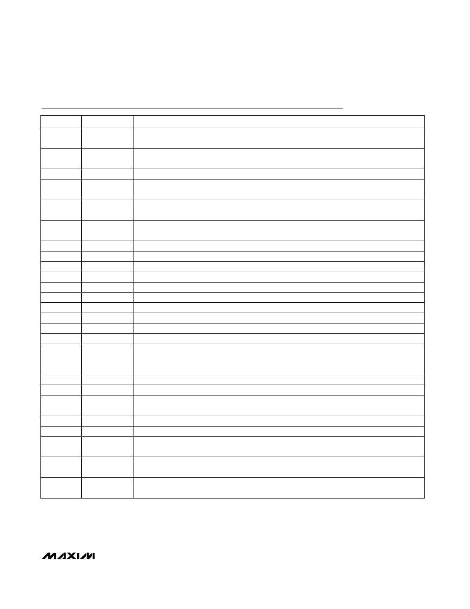
PIN
NAME
FUNCTION
1
AIN+
Positive Analog Input. Positive side of fully differential analog input. Bypass AIN+ to GND with a
0.1µF or greater capacitor.
2
AIN-
Negative Analog Input. Negative side of fully differential analog input. Bypass AIN- to GND with a
0.1µF or greater capacitor.
3
GND
Ground. Connect to star ground.
4
AV
DD
Analog Positive Supply Voltage. Connect AV
DD
to a +2.7V to +5.25V power supply. Bypass AV
DD
to GND with a 0.1µF capacitor.
5
DV
DD
Digital Positive Supply Voltage. Connect DV
DD
to a +2.7V to +5.25V power supply. Bypass DV
DD
to GND with a 0.1µF capacitor.
6
SET
Segment Current Set. Connect to ground through a resistor to set the segment current. See Table
7 for segment-current selection.
7
REG_VDD
V/I Converter Regulated Supply Output (5.2V typ)
8
REG_FORCE
REG_VDD Control. Drives the gate of external depletion-mode FET.
9
REG_AMP
Regulator/Reference Buffer Supply. Connect to a 4.75V to 5.25V power supply.
10
CMP
Regulator Compensation Node. Connect a 0.1µF capacitor from CMP to REG_FORCE.
11
DAC_VDD
DAC Analog Supply. Connect DAC_VDD to a +2.7V to +5.25V power supply.
12
DACVOUT
DAC Voltage Output. DAC output impedance is typically 6.2k
Ω.
13
CONV_IN
V/I Converter Input
14
4-20OUT
4–20mA (0 to 16mA) Current-Loop Output. Referenced to GND.
15
GND_DAC
DAC Analog Ground. Connect to star ground.
16
GND_V/I
V/I Converter Analog Ground. Connect to star ground.
17
REF_DAC
V-to-I Converter/DAC Reference Input. Connect a voltage source for external reference operation
or leave floating for internal reference. Bypass REF_DAC with a 0.1µF capacitor to GND for either
internal or external reference operation.
18
EN_BPM
Acti ve- H i g h V /I- C onver ter Bi p ol ar - M od e E nab l e. S et hi g h for b i p ol ar m od e. S et l ow for uni p ol ar m od e.
19
EN_I
Acti ve- H i g h V /I- C onver ter 4m A O ffset E nab l e. S et l ow for 0 to 16m A outp ut. S et hi g h for 4–20m A.
20
REFSELE
DAC External Reference Selection. Set low for internal reference. Set high for external reference.
Leave REF_DAC unconnected when REFSELE is low.
21
DACDATA_SEL
DAC Data-Source Select. Connect to logic high for the MAX1365/MAX1367.
22
CS_DAC
DAC Chip Select. Connect to logic high for the MAX1365/MAX1367.
23
INTREF
ADC Reference Selection. Set INTREF high to select the internal ADC reference. Set INTREF low
to select external ADC reference.
24
RANGE
ADC Range Select. Set RANGE low for
±2V analog input voltage range. Set RANGE high for
±200mV analog input voltage range.
25
PEAK
Peak Logic Input. Connect PEAK to DV
DD
to display the highest ADC value on the LED. Connect
PEAK to GND to disable the PEAK function (see Table 1).
Pin Description