Electrical characteristics (continued) – Rainbow Electronics MAX1215 User Manual
Page 4
MAX1215
1.8V, 12-Bit, 250Msps ADC for
Broadband Applications
4
_______________________________________________________________________________________
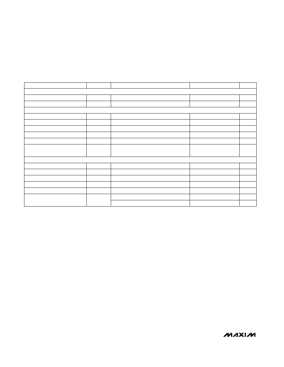
ELECTRICAL CHARACTERISTICS (continued)
(AV
CC
= OV
CC
= 1.8V, AGND = OGND = 0, f
SAMPLE
= 250MHz, differential sine-wave clock input drive, 0.1µF capacitor on REFIO,
internal reference, digital output pins differential R
L
= 100
Ω ±1%, T
A
= T
MIN
to T
MAX
, unless otherwise noted. Typical values are at
T
A
= +25°C.) (Note 1)
PARAMETER
SYMBOL
CONDITIONS
MIN
TYP
MAX
UNITS
LVCMOS DIGITAL INPUTS (CLKDIV,
T/B)
Digital Input-Voltage Low
V
IL
0.2 x AV
CC
V
Digital Input-Voltage High
V
IH
0.8 x AV
CC
V
TIMING CHARACTERISTICS
CLK-to-Data Propagation Delay
t
PDL
Figure 4
1.75
ns
CLK-to-DCLK Propagation Delay
t
CPDL
Figure 4
3.87
ns
DCLK-to-Data Propagation Delay
t
PDL
- t
CPDL
Figure 4 (Note 3)
1.66
2.12
2.48
ns
LVDS Output Rise Time
t
RISE
20% to 80%, C
L
= 5pF
460
ps
LVDS Output Fall Time
t
FALL
20% to 80%, C
L
= 5pF
460
ps
Output Data Pipeline Delay
t
LATENCY
Figure 4
11
Clock
cycles
POWER REQUIREMENTS
Analog Supply Voltage Range
AV
CC
1.70
1.80
1.90
V
Digital Supply Voltage Range
OV
CC
1.70
1.80
1.90
V
Analog Supply Current
I
AVCC
f
IN
= 100MHz
495
555
mA
Digital Supply Current
I
OVCC
f
IN
= 100MHz
64
75
mA
Analog Power Dissipation
P
DISS
f
IN
= 100MHz
1006
1134
mW
Offset
1.8
mV/V
Power-Supply Rejection Ratio
(Note 3)
PSRR
Gain
1.5
%FS/V
Note 1:
≥+25°C guaranteed by production test, <+25°C guaranteed by design and characterization.
Note 2: Static linearity and offset parameters are based on the end-point fit method. The full-scale range (FSR) is defined as 4095 x
slope of the line.
Note 3: Parameter guaranteed by design and characterization: T
A
= T
MIN
to T
MAX
.
Note 4: PSRR is measured with both analog and digital supplies connected to the same potential.