Rainbow Electronics MAX1215 User Manual
Page 11
MAX1215
1.8V, 12-Bit, 250Msps ADC for
Broadband Applications
______________________________________________________________________________________
11
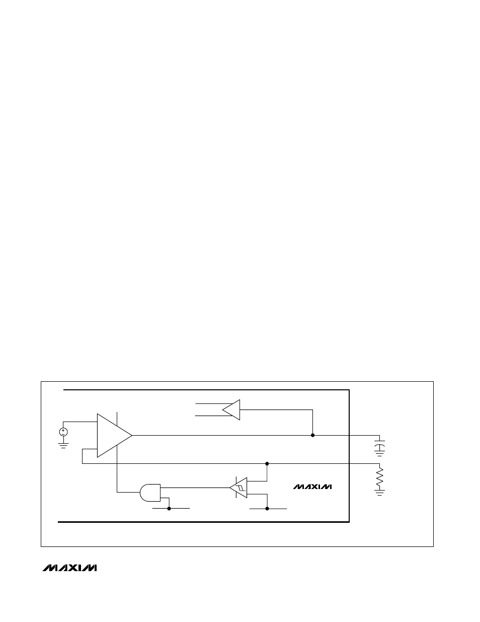
On-Chip Reference Circuit
The MAX1215 features an internal 1.23V bandgap refer-
ence circuit (Figure 3), which in combination with an inter-
nal reference-scaling amplifier determines the FSR of the
MAX1215. Bypass REFIO with a 0.1µF capacitor to
AGND. To compensate for gain errors or increase the
ADC’s FSR, the voltage of this bandgap reference can be
indirectly adjusted by adding an external resistor (e.g.,
100k
Ω trim potentiometer) between REFADJ and AGND
or REFADJ and REFIO. See the Applications Information
section for a detailed description of this process.
To disable the internal reference, connect REFADJ to
AV
CC
. In this configuration, an external, stable refer-
ence must be applied to REFIO to set the converter’s
full scale. To enable the internal reference, connect
REFADJ to AGND.
Clock Inputs (CLKP, CLKN)
Designed for a differential LVDS clock input drive, it is
recommended to drive the clock inputs of the MAX1215
with an LVDS- or LVPECL-compatible clock to achieve
the best dynamic performance. The clock signal source
must be a high-quality, low phase noise with fast edge
rates to avoid any degradation in the noise performance
of the ADC. The clock inputs (CLKP, CLKN) are internally
biased to 1.15V, accept a typical 0.5V
P-P
differential sig-
nal swing, and are usually driven in AC-coupled configu-
ration. See the Differential, AC-Coupled PECL-
Compatible Clock Input section for more circuit details
on how to drive CLKP and CLKN appropriately. Although
not recommended, the clock inputs also accept a single-
ended input signal.
The MAX1215 also features an internal clock-manage-
ment circuit (duty-cycle equalizer) that ensures the
clock signal applied to inputs CLKP and CLKN is
processed to provide a 50% duty-cycle clock signal
that desensitizes the performance of the converter to
variations in the duty cycle of the input clock source.
Note that the clock duty-cycle equalizer cannot be
turned off externally and requires a minimum clock fre-
quency of >20MHz to work appropriately and accord-
ing to data sheet specifications.
Data Clock Outputs (DCLKP, DCLKN)
The MAX1215 features a differential clock output, which
can be used to latch the digital output data with an
external latch or receiver. Additionally, the clock output
can be used to synchronize external devices (e.g.,
FPGAs) to the ADC. DCLKP and DCLKN are differential
outputs with LVDS-compatible voltage levels. There is a
3.87ns delay time between the rising (falling) edge of
CLKP (CLKN) and the rising edge of DCLKP (DCLKN).
See Figure 4 for timing details.
Divide-by-2 Clock Control (CLKDIV)
The MAX1215 offers a clock control line (CLKDIV),
which supports the reduction of clock jitter in a system.
Connect CLKDIV to OGND to enable the ADC’s internal
divide-by-2 clock divider. Data is now updated at one-
half the ADC’s input clock rate. CLKDIV has an internal
pulldown resistor and can be left open for applications
that require this divide-by-2 mode. Connecting CLKDIV
to OV
CC
disables the divide-by-2 mode.
MAX1215
REFERENCE
BUFFER
ADC FULL SCALE = REFT - REFB
REFT: TOP OF REFERENCE LADDER.
REFB: BOTTOM OF REFERENCE LADDER.
1V
AV
CC
AV
CC
/2
G
CONTROL LINE TO
DISABLE REFERENCE BUFFER
REFERENCE
SCALING AMPLIFIER
REFIO
REFADJ
0.1
µF
100
Ω*
*REFADJ MAY
BE SHORTED TO
AGND DIRECTLY
REFT
REFB
Figure 3. Simplified Reference Architecture