Rainbow Electronics MAX1215 User Manual
Page 14
MAX1215
1.8V, 12-Bit, 250Msps ADC for
Broadband Applications
14
______________________________________________________________________________________
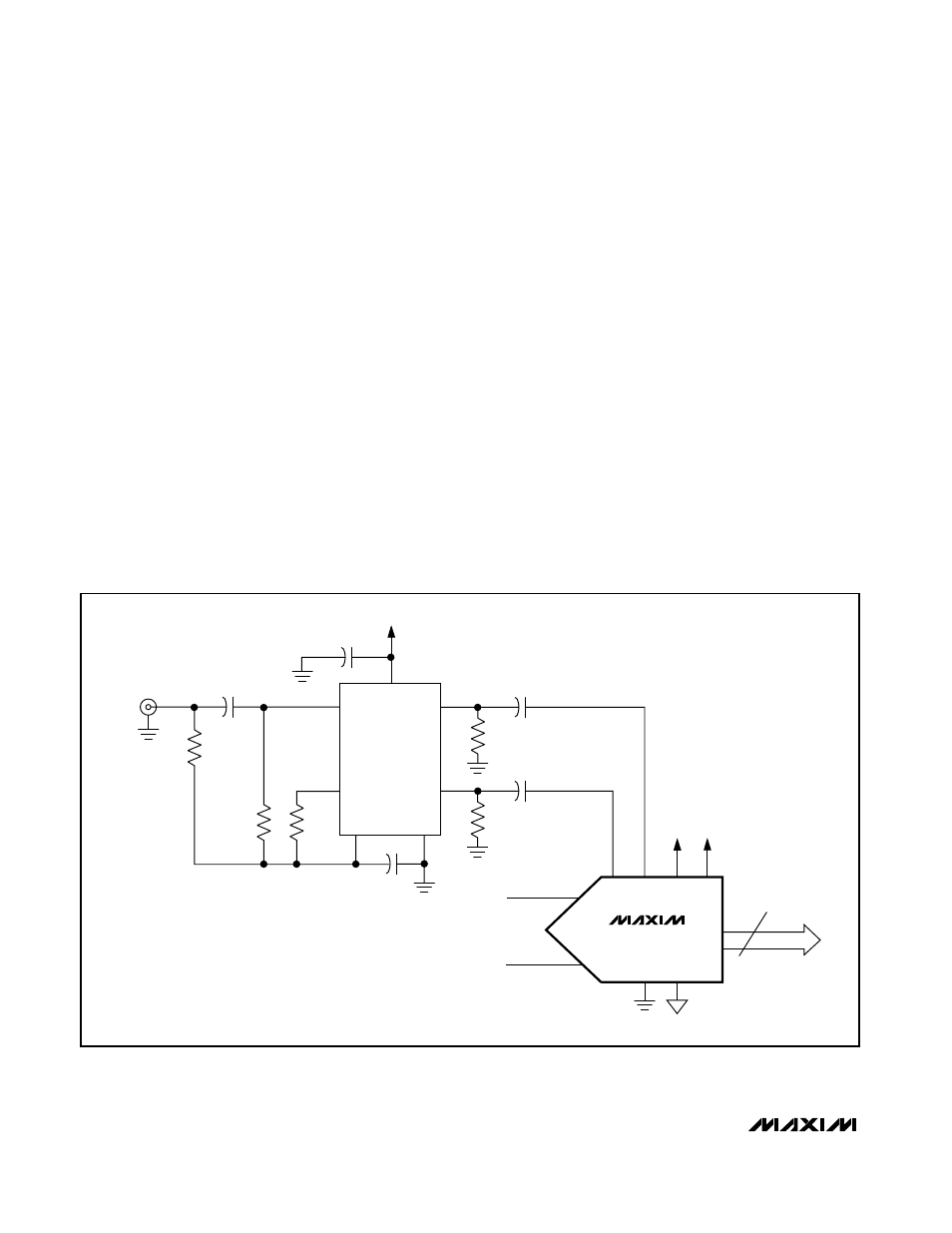
Differential, AC-Coupled, LVPECL-Compatible
Clock Input
The MAX1215 dynamic performance depends on the
use of a very clean clock source. The phase noise floor
of the clock source has a negative impact on the SNR
performance. Spurious signals on the clock signal
source also affect the ADC’s dynamic range. The pre-
ferred method of clocking the MAX1215 is differentially
with LVDS- or LVPECL-compatible input levels. The fast
data transition rates of these logic families minimize the
clock input circuitry’s transition uncertainty, thereby
improving the SNR performance. To accomplish this, a
50
Ω reverse-terminated clock signal source with low
phase noise is AC-coupled into a fast differential
receiver such as the MC100LVEL16D (Figure 7). The
receiver produces the necessary LVPECL output levels
to drive the clock inputs of the data converter.
Transformer-Coupled, Differential Analog
Input Drive
In general, the MAX1215 provides the best SFDR and
THD with fully differential input signals and it is not re-
commended to drive the ADC inputs in single-ended
configuration. In differential input mode, even-order
harmonics are usually lower since INP and INN are bal-
anced, and each of the ADC inputs only requires half
the signal swing compared to a single-ended configu-
ration. Wideband RF transformers provide an excellent
solution to convert a single-ended signal to a fully dif-
ferential signal, required by the MAX1215 to reach its
optimum dynamic performance.
A secondary-side termination of a 1:1 transformer (e.g.,
Mini-Circuit’s ADT1-1WT) into two separate 24.9
Ω ±1%
resistors (use tight resistor tolerances to minimize
effects of imbalance; 0.5% would be an ideal choice)
placed between top/bottom and center tap of the trans-
former is recommended to maximize the ADC’s dynam-
ic range. This configuration optimizes THD and SFDR
performance of the ADC by reducing the effects of
transformer parasitics. However, the source imped-
ance combined with the shunt capacitance provided
by a PC board and the ADC’s parasitic capacitance
limit the ADC’s full-power input bandwidth to approxi-
mately 600MHz.
MC100LVEL16D
VGND
AGND OGND
D0P/N–D11P/N
AV
CC
V
CLK
0.1
µF
0.1
µF
0.1
µF
0.1
µF
0.01
µF
SINGLE-ENDED
INPUT TERMINAL
150
Ω
150
Ω
CLKP
CLKN
INP
INN
OV
CC
12
2
8
4
5
7
6
3
50
Ω
510
Ω
510
Ω
MAX1215
Figure 7. Differential, AC-Coupled, PECL-Compatible Clock Input Configuration