Rainbow Electronics MAX1215 User Manual
Page 16
MAX1215
1.8V, 12-Bit, 250Msps ADC for
Broadband Applications
16
______________________________________________________________________________________
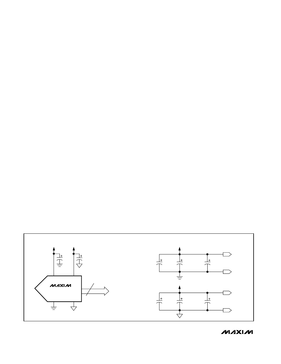
To achieve optimum performance, provide each supply
with a separate network of a 47µF tantalum capacitor
and parallel combinations of 10µF and 1µF ceramic
capacitors. Additionally, the ADC requires each supply
pin to be bypassed with separate 0.1µF ceramic
capacitors (Figure 10). Locate these capacitors directly
at the ADC supply pins or as close as possible to the
MAX1215. Choose surface-mount capacitors, whose
preferred location should be on the same side as the
converter to save space and minimize the inductance.
If close placement on the same side is not possible,
these bypassing capacitors may be routed through
vias to the bottom side of the PC board.
Multilayer boards with separated ground and power
planes produce the highest level of signal integrity.
Consider the use of a split ground plane arranged to
match the physical location of analog and digital
ground on the ADC’s package. The two ground planes
should be joined at a single point so the noisy digital
ground currents do not interfere with the analog ground
plane. The dynamic currents that may need to travel
long distances before they are recombined at a com-
mon-source ground, resulting in large and undesirable
ground loops, are a major concern with this approach.
Ground loops can degrade the input noise by coupling
back to the analog front-end of the converter, resulting
in increased spurious activity, leading to decreased
noise performance.
Alternatively, all ground pins could share the same
ground plane, if the ground plane is sufficiently isolated
from any noisy, digital systems ground. To minimize the
coupling of the digital output signals from the analog
input, segregate the digital output bus carefully from the
analog input circuitry. To further minimize the effects of
digital noise coupling, ground return vias can be posi-
tioned throughout the layout to divert digital switching
currents away from the sensitive analog sections of the
ADC. This approach does not require split ground
planes, but can be accomplished by placing substantial
ground connections between the analog front-end and
the digital outputs.
The MAX1215 is packaged in a 68-pin QFN-EP pack-
age (package code: G6800-4), providing greater
design flexibility, increased thermal dissipation, and
optimized AC performance of the ADC. The exposed
paddle (EP) must be soldered down to AGND.
In this package, the data converter die is attached to
an EP lead frame with the back of this frame exposed
at the package bottom surface, facing the PC board
side of the package. This allows a solid attachment of
the package to the board with standard infrared (IR)
flow soldering techniques.
Thermal efficiency is one of the factors for selecting a
package with an exposed pad for the MAX1215. The
exposed pad improves thermal and ensures a solid
ground connection between the DAC and the PC
board’s analog ground layer.
Considerable care must be taken when routing the digi-
tal output traces for a high-speed, high-resolution data
converter. It is recommended running the LVDS output
traces as differential lines with 100
Ω matched imped-
ance from the ADC to the LVDS load device.
AGND
NOTE: EACH POWER-SUPPLY PIN (ANALOG
AND DIGITAL) SHOULD BE DECOUPLED WITH
AN INDIVIDUAL 0.1
µF CAPACITOR AS CLOSE
AS POSSIBLE TO THE ADC.
BYPASSING—ADC LEVEL
BYPASSING—BOARD LEVEL
ANALOG POWER-
SUPPLY SOURCE
OGND
AGND
OGND
D0P/N–D11P/N
1
µF
10
µF
0.1
µF
0.1
µF
47
µF
AV
CC
OV
CC
12
MAX1215
AV
CC
DIGITAL/OUTPUT
DRIVER POWER-
SUPPLY SOURCE
1
µF
10
µF
47
µF
OV
CC
Figure 10. Grounding, Bypassing, and Decoupling Recommendations for the MAX1215