Detailed description— theory of operation, Analog inputs (inp, inn) – Rainbow Electronics MAX1215 User Manual
Page 10
MAX1215
1.8V, 12-Bit, 250Msps ADC for
Broadband Applications
10
______________________________________________________________________________________
Detailed Description—
Theory of Operation
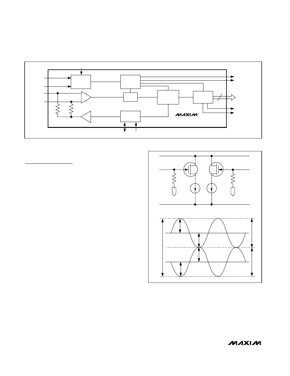
The MAX1215 uses a fully differential pipelined archi-
tecture that allows for high-speed conversion, opti-
mized accuracy, and linearity while minimizing power
consumption and die size.
Both positive (INP) and negative/complementary ana-
log input terminals (INN) are centered around a 1.365V
common-mode voltage, and accept a differential ana-
log input voltage swing of
±V
FS
/ 4V each, resulting in a
typical 1.454V
P-P
differential full-scale signal swing.
Inputs INP and INN are buffered prior to entering each
T/H stage and are sampled when the differential sam-
pling clock signal transitions high.
Each pipeline converter stage converts its input voltage
to a digital output code. At every stage, except the last,
the error between the input voltage and the digital out-
put code is multiplied and passed along to the next
pipeline stage. Digital error correction compensates for
ADC comparator offsets in each pipeline stage and
ensures no missing codes. The result is a 12-bit parallel
digital output word in user-selectable two’s-complement
or offset binary output formats with LVDS-compatible
output levels. See Figure 1 for a more detailed view of
the MAX1215 architecture.
Analog Inputs (INP, INN)
INP and INN are the fully differential inputs of the
MAX1215. Differential inputs usually feature good rejec-
tion of even-order harmonics, which allows for
enhanced AC performance as the signals are progress-
ing through the analog stages. The MAX1215 analog
inputs are self-biased at a 1.365V common-mode volt-
age and allow a 1.454V
P-P
differential input voltage
swing (Figure 2). Both inputs are self-biased through
2k
Ω resistors, resulting in a typical differential input
resistance of 4k
Ω. It is recommended to drive the ana-
log inputs of the MAX1215 in AC-coupled configuration
to achieve best dynamic performance. See the
Transformer-Coupled, Differential Analog Input Drive
section for a detailed discussion of this configuration.
MAX1215
CLOCK-
DIVIDER
CONTROL
CLKDIV
CLOCK
MANAGEMENT
INPUT
BUFFER
DCLKP
D0P/N–D11P/N
DCLKN
12
ORP
ORN
2.2k
Ω
2.2k
Ω
CLKP
CLKN
INP
INN
COMMON-MODE
BUFFER
REFIO
REFADJ
LVDS
DATA PORT
REFERENCE
T/H
12-BIT PIPELINE
QUANTIZER
CORE
2.2k
Ω
INP
2.2k
Ω
AGND
COMMON-MODE
VOLTAGE (1.365V)
COMMON-MODE
VOLTAGE (1.365V)
INN
TO COMMON MODE
TO COMMON MODE
1.454V
P-P
DIFFERENTIAL FSR
INP
INN
AV
CC
-V
FS
/
4
+V
FS
/
4
-V
FS
/
4
+V
FS
/
4
V
FS
/
2
V
FS
/
2
Figure 1. MAX1215 Block Diagram
Figure 2. Simplified Analog Input Architecture and Allowable
Input Voltage Range