Applications information – Rainbow Electronics MAX1215 User Manual
Page 13
MAX1215
1.8V, 12-Bit, 250Msps ADC for
Broadband Applications
______________________________________________________________________________________
13
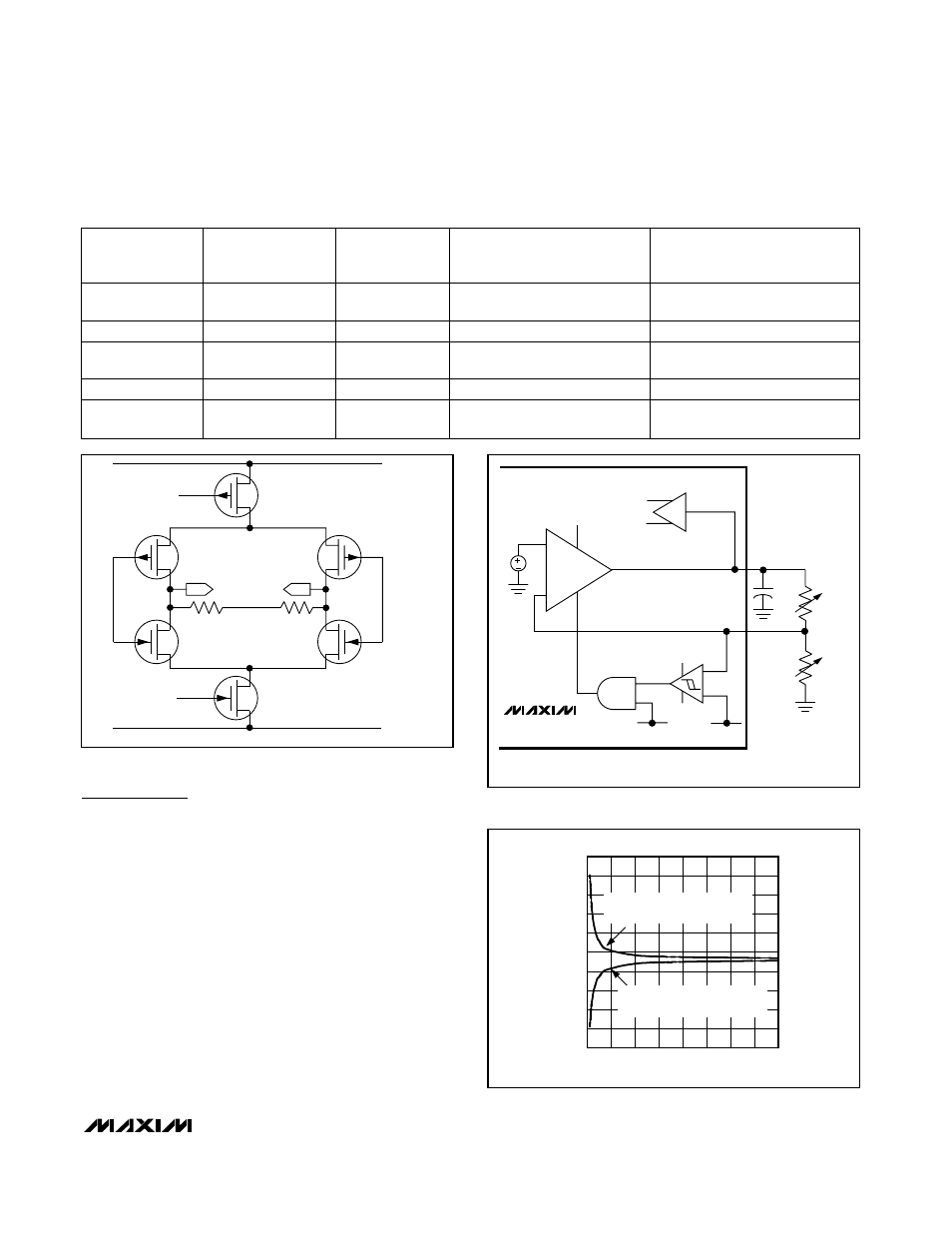
Applications Information
FSR Adjustments Using the Internal
Bandgap Reference
The MAX1215 supports a full-scale adjustment range of
10% (±5%). To decrease the full-scale signal range, an
external resistor value ranging from 13k
Ω to 1MΩ may
be added between REFADJ and AGND. A similar
approach can be taken to increase the ADC’s full-scale
range (FSR). Adding a variable resistor, potentiometer,
or predetermined resistor value between REFADJ and
REFIO increases the FSR of the data converter. Figure
6a shows the two possible configurations and their
impact on the overall full-scale range adjustment of the
MAX1215. Do not use resistor values of less than 13k
Ω
to avoid instability of the internal gain regulation loop
for the bandgap reference. See Figure 6b for the
results of the adjustment range for a selection of resis-
tors used to trim the full-scale range of the MAX1215.
Table 1. MAX1215 Digital Output Coding
INP ANALOG
INPUT VOLTAGE
LEVEL
INN ANALOG
INPUT VOLTAGE
LEVEL
OUT-OF-RANGE
ORP (ORN)
BINARY DIGITAL OUTPUT
CODE (D11P/N–D0P/N)
TWO’S COMPLEMENT DIGITAL
OUTPUT CODE (D11P/N–D0P/N)
> V
CM
+ V
FS
/ 4
< V
CM
- V
FS
/ 4
1 (0)
1111 1111 1111
(exceeds +FS, OR set)
0111 1111 1111
(exceeds +FS, OR set)
V
CM
+ V
FS
/ 4
V
CM
- V
FS
/ 4
0 (1)
1111 1111 1111 (+FS)
0111 1111 1111 (+FS)
V
CM
V
CM
0 (1)
1000 0000 0000 or
0111 1111 1111 (FS/2)
0000 0000 0000 or
1111 1111 1111 (FS/2)
V
CM
- V
FS
/ 4
V
CM
+ V
FS
/ 4
0 (1)
0000 0000 0000 (-FS)
1000 0000 0000 (-FS)
< V
CM
+ V
FS
/ 4
> V
CM
- V
FS
/ 4
1 (0)
00 0000 0000
(exceeds -FS, OR set)
10 0000 0000
(exceeds -FS, OR set)
V
ON
OGND
OV
CC
V
OP
2.2k
Ω
2.2k
Ω
Figure 5. Simplified LVDS Output Architecture
MAX1215
REFERENCE
BUFFER
ADC FULL SCALE = REFT - REFB
REFT: TOP OF REFERENCE LADDER.
REFB: BOTTOM OF REFERENCE LADDER.
1V
AV
CC
AV
CC
/2
G
CONTROL LINE
TO DISABLE
REFERENCE BUFFER
REFERENCE-
SCALING
AMPLIFIER
REFIO
REFADJ
13k
Ω TO
1M
Ω
0.1
µF
REFT
REFB
13k
Ω TO
1M
Ω
Figure 6a. Circuit Suggestions to Adjust the ADC’s Full-Scale
Range
FS VOLTAGE vs. FS ADJUST RESISTOR
MAX1213 fig06b
FS ADJUST RESISTOR (
Ω)
V
FS
(V)
875
750
500 625
250 375
125
1.39
1.41
1.43
1.45
1.47
1.49
1.51
1.53
1.55
1.57
1.37
0
1000
RESISTOR VALUE APPLIED BETWEEN
REFADJ AND REFIO INCREASES V
FS
RESISTOR VALUE APPLIED BETWEEN
REFADJ AND AGND DECREASES V
FS
Figure 6b. FS Adjustment Range vs. FS Adjustment Resistor