Detailed description, Pin description, Timing – Rainbow Electronics MAX909 User Manual
Page 8
MAX907/MAX908/MAX909
_______________Detailed Description
Timing
Noise or undesired parasitic AC feedback cause most
high-speed comparators to oscillate in the linear region
(i.e., when the voltage on one input is at or near the
voltage on the other input). The MAX907/MAX908/
MAX909 eliminate this problem by incorporating inter-
nal hysteresis. When the two comparator input voltages
are equal, hysteresis effectively causes one comparator
input voltage to move quickly past the other, thus taking
the input out of the region where oscillation occurs.
Standard comparators require that hysteresis be added
through the use of external resistors. The
MAX907/MAX908/MAX909’s fixed internal hysteresis
eliminates these resistors (and the equations required
to determine appropriate values).
Adding hysteresis to a comparator creates two trip
points: one for the input voltage rising and one for the
input voltage falling (Figure 1). The difference between
these two input-referred trip points is the hysteresis.
Figure 1 illustrates the case where IN- is fixed and IN+
is varied. If the inputs were reversed, the figure would
look the same, except the output would be inverted.
The MAX909 includes an internal latch, allowing the
result of a comparison to be stored. If LE is low, the
latch is transparent (i.e., the comparator operates as
though the latch is not present). The state of the com-
parator output is stored when LE is high (Figure 2).
Note that the MAX909 can be operated with V- con-
nected to ground or to a negative supply voltage. The
MAX909’s input range extends from (V- - 0.2V) to
(V+ - 1.5V).
Dual/Quad/Single, High-Speed, Ultra-Low-Power,
Single-Supply TTL Comparators
8
_______________________________________________________________________________________
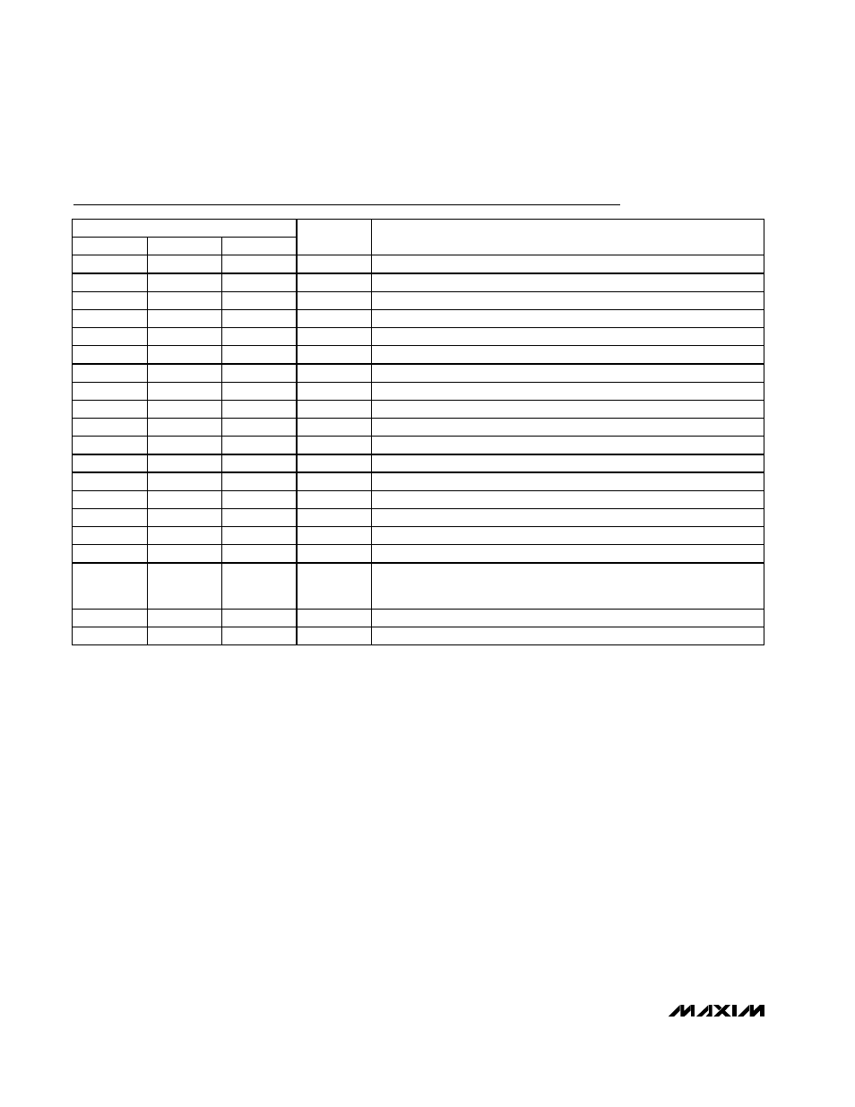
Pin Description
PIN
NAME
FUNCTION
MAX907
MAX908
MAX909
1
1
—
OUTA
Comparator A Output
2
2
—
INA-
Comparator A Inverting Input
3
3
—
INA+
Comparator A Noninverting Input
4
11
6
GND
Ground
5
5
—
INB+
Comparator B Noninverting Input
6
6
—
INB-
Comparator B Inverting Input
7
7
—
OUTB
Comparator B Output
8
4
1
V+
Positive Supply
—
8
—
OUTC
Comparator C Output
—
9
—
INC-
Comparator C Inverting Input
—
10
—
INC+
Comparator C Noninverting Input
—
12
—
IND+
Comparator D Noninverting Input
—
13
—
IND-
Comparator D Inverting Input
—
14
—
OUTD
Comparator D Output
—
—
2
IN+
Noninverting Input
—
—
3
IN-
Inverting Input
—
—
4
V-
Negative Supply or Ground
—
—
5
LE
—
—
7
QOUT
Comparator Output
—
—
8
QOUT
Inverted Comparator Output
The latch is transparent when LE is low. The comparator output is
stored when LE is high.