Electrical characteristics, Absolute maximum ratings – Rainbow Electronics MAX909 User Manual
Page 2
MAX907/MAX908/MAX909
Dual/Quad/Single, High-Speed, Ultra-Low-Power,
Single-Supply TTL Comparators
2
_______________________________________________________________________________________
Positive Supply Voltage (V+ to GND) . . . . . . . . . . . . . . . . . . . . . . . . +6V
Negative Supply Voltage (V- to GND, MAX909 only) . . . . . . . . . -7V
Differential Input Voltage
MAX907/MAX908 . . . . . . . . . . . . . . . . . . . . . . . . . . -0.3V to (V+ + 0.3V)
MAX909 . . . . . . . . . . . . . . . . . . . . . . . . . . . . . . (V- - 0.3V) to (V+ + 0.3V)
Common-Mode Input Voltage
MAX907/MAX908 . . . . . . . . . . . . . . . . . . . . . . . . . . -0.3V to (V+ + 0.3V)
MAX909 . . . . . . . . . . . . . . . . . . . . . . . . . . . . . . (V- - 0.3V) to (V+ + 0.3V)
Latch Input Voltage (MAX909 only) . . . . . . . . . -0.3V to (V+ + 0.3V)
Input/Output Short-Circuit Duration to V+ or GND . . . Continuous
Continuous Power Dissipation (T
A
= +70°C)
8-Pin Plastic DIP (derate 9.09mW/°C above +70°C) . . . 727mW
8-Pin SO (derate 5.88mW/°C above +70°C) . . . . . . . . . . . 471mW
14-Pin Plastic DIP (derate 10.00mW/°C above +70°C) . . . 800mW
14-Pin SO (derate 8.33mW/°C above +70°C) . . . . . . . . . . 667mW
Operating Temperature Ranges:
MAX90_C_ _ . . . . . . . . . . . . . . . . . . . . . . . . . . . . . . . . . . . . . . 0°C to +70°C
MAX90_E_ _ . . . . . . . . . . . . . . . . . . . . . . . . . . . . . . . . . . . -40°C to +85°C
Storage Temperature Range . . . . . . . . . . . . . . . . . . . -65°C to +150°C
Lead Temperature (soldering, 10s) . . . . . . . . . . . . . . . . . . . . . . +300°C
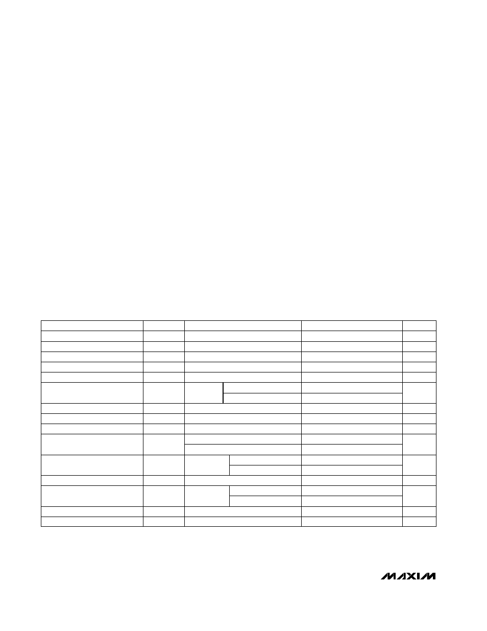
ELECTRICAL CHARACTERISTICS
(V+ = 5V, T
A
= +25°C; MAX909 only: V- = 0, V
LATCH
= 0; unless otherwise noted.)
Stresses beyond those listed under “Absolute Maximum Ratings" may cause permanent damage to the device. These are stress ratings only, and functional
operation of the device at these or any other conditions beyond those indicated in the operational sections of the specifications is not implied. Exposure to
absolute maximum rating conditions for extended periods may affect device reliability.
ABSOLUTE MAXIMUM RATINGS
PARAMETER
CONDITIONS
MIN
TYP
MAX
UNITS
Positive Trip Point
V
TRIP+
(Note 1)
2
4
mV
Negative Trip Point
V
TRIP-
(Note 1)
-2
-4
mV
Input Offset Voltage
V
OS
(Note 2)
0.5
2.0
mV
Input Bias Current
I
B
V
CM
= 0, V
IN
= V
OS
100
300
nA
Input Offset Current
I
OS
V
CM
= 0, V
IN
= V
OS
25
50
nA
Input Voltage Range
V
CMR
-0.2
V+ - 1.5
V
-5.2
V+ - 1.5
Common-Mode Rejection Ratio
CMRR
(Notes 4, 5)
50
100
µV/V
Power-Supply Rejection Ratio
PSRR
(Notes 4, 6)
50
100
µV/V
Output High Voltage
V
OH
I
SOURCE
= 100µA
3.0
3.5
V
Output Low Voltage
V
OL
I
SINK
= 3.2mA
0.3
0.4
I
SINK
= 8mA
0.4
Positive Supply Current per
Comparator
I+
(Note 7)
0.7
1.0
mA
1.2
1.8
Negative Supply Current
I-
MAX909 only: V- = -5V
60
100
µA
Power Dissipation per
Comparator
PD
(Note 8)
3.5
5.5
mW
6
10
Output Rise Time
t
r
12
ns
Output Fall Time
t
f
6
ns
SYMBOL
MAX907/MAX908/MAX909
MAX907/MAX908
MAX909
MAX909
(Notes 3, 4)
MAX907/MAX908
V
OUT
= 0.4V to 2.4V, C
L
= 10pF
V
OUT
= 2.4V to 0.4V, C
L
= 10pF
V
MAX909 only: V- = -5V