Electrical characteristics (continued) – Rainbow Electronics MAX909 User Manual
Page 4
MAX907/MAX908/MAX909
Dual/Quad/Single, High-Speed, Ultra-Low-Power,
Single-Supply TTL Comparators
4
_______________________________________________________________________________________
Note 1:
Trip Point is defined as the input voltage required to make the comparator output change state. The difference
between upper (V
TRIP
+) and lower (V
TRIP
-) trip points is equal to the width of the input-referred hysteresis zone (V
HYST
).
Specified for an input common-mode voltage (V
CM
) of 0 (see Figure 1).
Note 2:
Input Offset Voltage is defined as the center of the input-referred hysteresis zone. Specified for V
CM
= 0 (see Figure 1).
Note 3:
Inferred from the CMRR test. Note that a correct logic result is obtained at the output, provided that at least one input is
within the V
CMR
limits. Note also that either or both inputs can be driven to the upper or lower absolute maximum limit with-
out damage to the part.
Note 4:
Tested with V+ = 5.5V (and V- = 0 for MAX909). MAX909 also tested over the full analog input range (i.e., with
V- = -5.5V).
Note 5:
Tested over the full input voltage range (V
CMR
).
Note 6:
Specified over the full tolerance of operating supply voltage: MAX907/MAX908 tested with 4.5V < V+ < 5.5V. MAX909
tested with 4.5V < V+ < 5.5V and with -5.5V < V- < 0.
Note 7:
Positive Supply Current specified with the worst-case condition of all outputs at logic low (MAX907/MAX908), and
with V+ = 5.5V.
Note 8:
Typical power specified with V+ = 5V; maximum with V+ = 5.5V (and with V- = -5.5V for MAX909).
Note 9:
Due to difficulties in measuring propagation delay with 5mV of overdrive in automatic test equipment, the
MAX907/MAX908/MAX909 are sample tested to 0.1% AQL with 100mV input overdrive. Correlation tests show that the
specification can be guaranteed if all other DC parameters are within the specified limits. V
OS
must be added to the over-
drive voltage for low values of overdrive.
Note 10: Differential Propagation Delay is specified as the difference between any two channels in the MAX907/MAX908 (both out-
puts making either a low-to-high or a high-to-low transition).
Note 11: Propagation Delay Skew is specified as the difference between any single channel’s output low-to-high transition (t
PD
+)
and high-to-low transition (t
PD
-), and also between the QOUT and QOUT transition on the MAX909.
Note 12: Latch specifications apply to MAX909 only (see Figure 2).
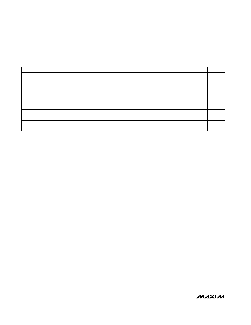
ELECTRICAL CHARACTERISTICS (continued)
(V+ = 5V, T
A
= T
MIN
to T
MAX
; MAX909 only: V- = 0, V
LATCH
= 0; unless otherwise noted.)
PARAMETER
SYMBOL
CONDITIONS
MIN
TYP
MAX
UNITS
Propagation Delay
t
PD+,
t
PD-
V
IN
= 100mV, V
OD
= 5mV
(Note 9)
45
70
ns
Differential Propagation Delay
∆t
PD
V
IN
= 100mV, V
OD
= 5mV
(Note 10)
2
ns
Propagation Delay Skew
t
PD
skew
MAX909 only: V
IN
= 100mV,
V
OD
= 5mV (Note 11)
4
ns
Latch Input Voltage High
V
IH
(Note 12)
2.0
V
Latch Hold Time
t
h
(Note 12)
4
ns
Latch Input Voltage Low
V
IL
(Note 12)
0.8
V
Latch Input Current
I
IH
, I
IL
(Note 12)
20
µA
Latch Setup Time
t
s
(Note 12)
4
ns