Rainbow Electronics MAX552 User Manual
Page 9
symmetrical, then the clock signal used must meet the
t
CH
and t
CL
requirements given in the
Electrical
Characteristics
.
Figure 2 shows the MAX551/MAX552 timing diagram.
The most significant bit (MSB) is always loaded first on
SCLK’s rising edge. When all data is shifted into the
input register, the DAC register is loaded by driving the
LOAD signal low. The DAC register is transparent when
LOAD is low and latched when LOAD is high. The
MAX551/MAX552 digital inputs are compatible with
CMOS logic levels. The MAX551’s inputs are also com-
patible with TTL logic.
Unipolar Operation
Figure 3 shows the MAX551/MAX552’s basic applica-
tion. This circuit is used for unipolar operation or 2-
quadrant multiplication. The code table for this mode is
given in Table 1. Note that the output’s polarity is the
opposite of the reference voltage polarity.
In many applications the gain accuracy is sufficient and
gain adjustment is not necessary. In these cases, resis-
tors R1 and R2 in Figure 3 can be omitted. If the gain is
trimmed and the DAC is operated over a wide tempera-
ture range, use low-tempco (<300ppm/°C) resistors for
R1 and R2. Capacitor C1 provides phase compensa-
tion and reduces overshoot and ringing when fast
amplifiers are used at the DAC’s output.
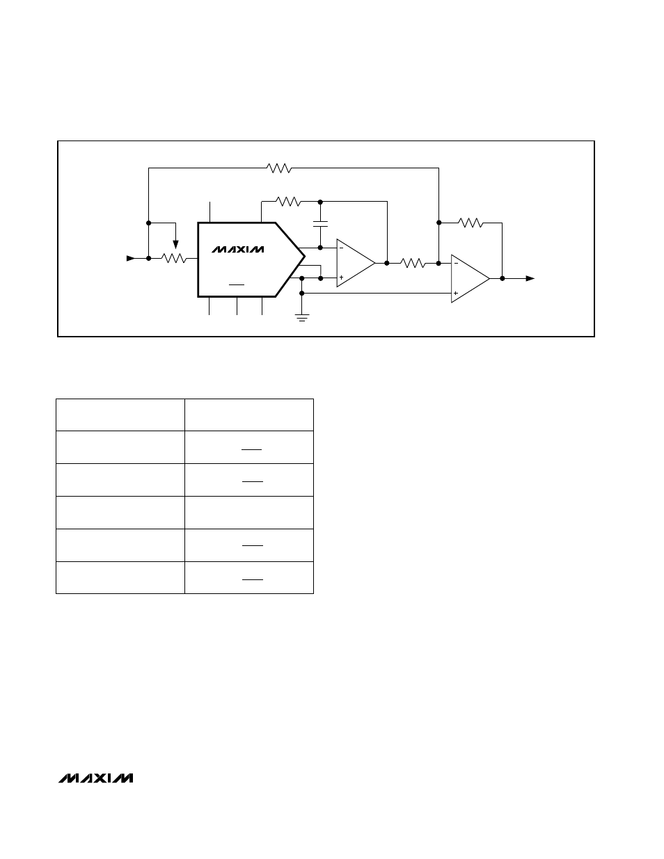
Bipolar Operation
Figure 4 shows the MAX551/MAX552 operating in bipo-
lar (or 4-quadrant multiplying) mode. Matched resistors
R3, R4, and R5 must be of the same material (prefer-
ably metal film or wire-wound) for good temperature-
tracking characteristics (<15ppm/°C) and should
match to 0.01% for 12-bit performance. The output
code is offset binary, as listed in Table 2.
To adjust the circuit, load the DAC with a code of 1000
0000 0000 and trim R1 for a 0V output. With R1 and R2
omitted, an alternative zero trim is needed to adjust the
ratio of R3 and R4 for 0V out. Trim full scale by loading
the DAC with all 0s or 1s and adjusting the V
REF
ampli-
tude or varying R5 until the desired positive or negative
output is obtained. In applications where gain trim is
not required, omit resistors R1 and R2. If gain trim is
desired and the DAC is operated over a wide tempera-
MAX551/MAX552
+3V/+5V, 12-Bit, Serial, Multiplying DACs
in 10-Pin µMAX Package
_______________________________________________________________________________________
9
Table 2. Offset Binary-Code Table
for Circuit of Figure 4
MAX551
MAX552
R3
10k
C1
33pF
+5V (+3V)
V
DD
V
REF
RFB
GND
SCLK
LOAD
DIN
AGND
REF
OUT
R2
50
Ω
R4
20k
R1
100
Ω
R5
20k
V
OUT
( ) ARE FOR MAX552
DIGITAL INPUT
MSB
LSB
ANALOG OUTPUT
1 1 1 1
1 1 1 1
1 1 1 1
1000
0000
0001
1 0 0 0
0 0 0 0
0 0 0 0
0 1 1 1
1 1 1 1
1 1 1 1
Figure 4. Bipolar Operation
0 0 0 0
0 0 0 0
0 0 0 0
+
V
REF
2047
2048
+
V
REF
1
2048
0
−
V
REF
1
2048
−
V
REF
2048
2048