Rainbow Electronics MAX552 User Manual
Page 2
MAX551/MAX552
+3V/+5V, 12-Bit, Serial, Multiplying DACs
in 10-Pin µMAX Package
2
_______________________________________________________________________________________
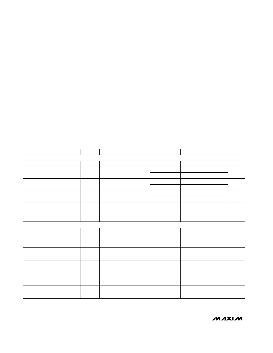
ABSOLUTE MAXIMUM RATINGS
ELECTRICAL CHARACTERISTICS—MAX551
(V
DD
= +4.5V to +5.25V, V
REF
= 5V, OUT = AGND = GND, T
A
= T
MIN
to T
MAX
, unless otherwise noted. Typical values are at
T
A
= +25°C.) (Note 1)
Stresses beyond those listed under “Absolute Maximum Ratings” may cause permanent damage to the device. These are stress ratings only, and functional
operation of the device at these or any other conditions beyond those indicated in the operational sections of the specifications is not implied. Exposure to
absolute maximum rating conditions for extended periods may affect device reliability.
V
DD
to GND..............................................................................6V
REF, RFB to GND.................................................................±12V
Digital Inputs (SCLK, DIN, LOAD, CLR)
to GND .....................................................................-0.3V to 6V
OUT to GND ...............................................-0.3V to (V
DD
+ 0.3V)
AGND to GND ............................................-0.3V to (V
DD
+ 0.3V)
Continuous Power Dissipation (T
A
= +70°C)
Plastic DIP (derate 9.09mW/°C above +70°C) .............727mW
µMAX (derate 5.60mW/°C above +70°C) .....................444mW
Operating Temperature Ranges
MAX55_ _C_ _......................................................0°C to +70°C
MAX55_ _E_ _ ...................................................-40°C to +85°C
Storage Temperature Range .............................-65°C to +150°C
Lead Temperature (soldering, 10sec) .............................+300°C
V
REF
= 6V
RMS
at 1kHz, DAC register loaded
with all 1s
V
REF
= 5Vp-p at 10kHz, DAC register loaded
with all 0s
Using internal feedback resistor (R
FB
)
(Note 2)
∆
V
DD
= +5%, -10%
T
A
= +25°C, to 1/2LSB, OUT load is
100
Ω
||13pF, DAC register alternately loaded
with 1s and 0s
10Hz to 100kHz, measured between RFB and
OUT
CONDITIONS
nV/
√
Hz
13
15
Output Noise-Voltage Density
±1
Gain Error
LSB
±1/2
INL
dB
-85
THD
Total Harmonic Distortion
mVp-p
0.3
1
AC Feedthrough at OUT
µs
0.08
1
ppm/°C
±0.2
±1
Gain Tempco
(
∆
Gain/
∆
Temp)
ppm/%
2
PSR
Power-Supply Rejection
t
S
Current Settling Time
UNITS
MIN
TYP
MAX
SYMBOL
PARAMETER
MAX551A
Bits
12
N
Resolution
MAX551B
±1
Integral Nonlinearity
Guaranteed monotonic over
temperature
MAX551A
±1/2
DNL
Differential Nonlinearity
MAX551B
±1
MAX551A
MAX551B
Using internal feedback
resistor (R
FB
)
±2
V
REF
= 0V, OUT load is 100
Ω
||13pF, DAC
register alternately loaded with 1s and 0s
Digital-to-Analog Glitch
nV-s
0.65
20
STATIC PERFORMANCE
DYNAMIC PERFORMANCE
(Note 3)
LSB
LSB