Detailed description, Serial interface – Rainbow Electronics MAX552 User Manual
Page 8
MAX551/MAX552
+3V/+5V, 12-Bit, Serial, Multiplying DACs
in 10-Pin µMAX Package
8
_______________________________________________________________________________________
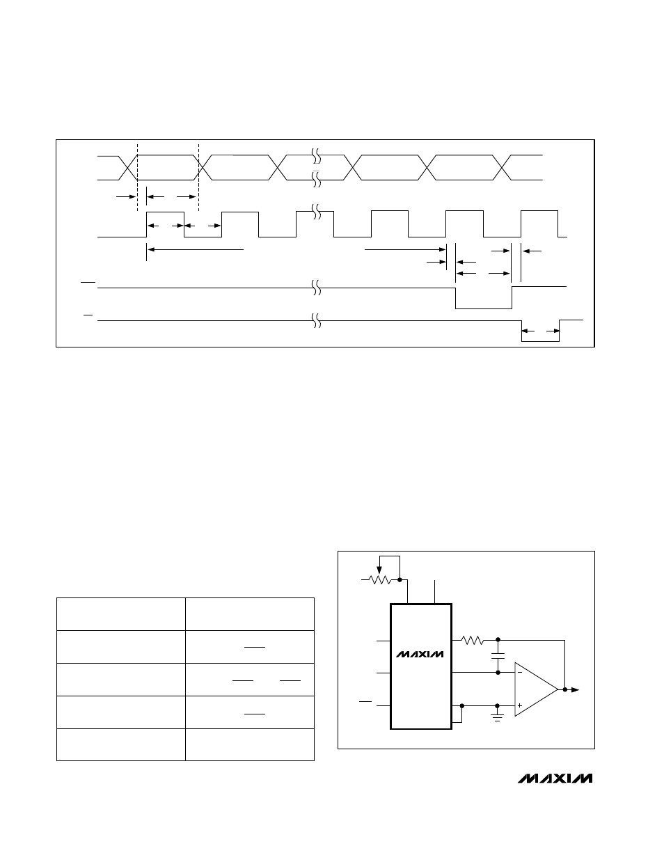
DIN
SCLK
LOAD
BIT 11
MSB
BIT 0
LSB
BIT 10
BIT 1
t
DS
t
DH
t
CH
1
2
LOAD SERIAL DATA INTO INPUT REGISTER
11
t
CL
t
CLR
t
SL
t
LD
t
LC
CLR
Figure 2. Write-Cycle Timing Diagram
MAX551
MAX552
+5V (+3V)
( ) ARE FOR MAX552
V
REF
V
DD
R2
50
Ω
C1
15pF
2
3
V
OUT
6
R1
100
Ω
DIN
REF
RFB
OUT
GND
AGND
SCLK
LOAD
Table 1. Unipolar Binary-Code Table
for Circuit of Figure 3
DIGITAL INPUT
MSB
LSB
ANALOG OUTPUT
1 1 1 1
1 1 1 1
1 1 1 1
1000
0000
0000
0 0 0 0
0 0 0 0
0 0 0 1
0 0 0 0
0 0 0 0
0 0 0 0
0
−
V
REF
4095
4096
−
= −
V
V
REF
REF
2048
4096
2
−
V
REF
1
4096
Figure 3. Unipolar Operation
Detailed Description
The MAX551/MAX552 digital-to-analog converter (DAC)
circuits consist of a laser-trimmed, thin-film R-2R resis-
tor array with NMOS current switches (Figure 1).
Binary-weighted currents are switched to either OUT or
AGND, depending on the status of each input data bit.
Although the currents at OUT and AGND depend on
the digital input code, the sum of the two output cur-
rents is always equal to the input current at REF.
The output current (I
OUT
) can be converted into a volt-
age by adding an external output amplifier (Figure 3).
The REF input accepts a wide range of signals, includ-
ing fixed and time-varying voltage or current inputs. If a
current source is used at the reference input, use a
low-tempco, external feedback resistor in place of the
internal feedback resistor (R
FB
) to minimize gain varia-
tion with temperature.
The internal feedback resistor (R
FB
) is compensated
with an NMOS switch that matches the NMOS switches
used in the R-2R array, resulting in excellent supply
rejection and gain-temperature coefficient.
The OUT pin output capacitance (C
OUT
) is code
dependent. C
OUT
is typically
14
pF at 000hex and
20
pF
at FFFhex.
Serial Interface
The MAX551/MAX552 serial interface is compatible
with the SPI/QSPI and Microwire serial-interface stan-
dards. These devices accept serial clocks up to
12.5MHz (50% duty cycle). If the SCLK input is not