Rainbow Electronics MAX552 User Manual
Page 11
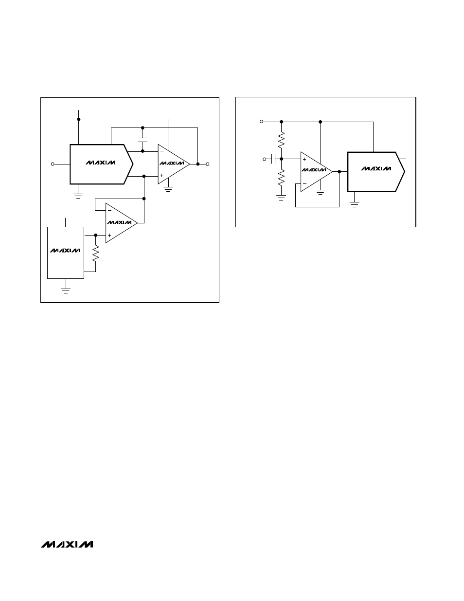
Figure 5 shows the MAX551 connected as a voltage
output DAC. In this mode of operation, the OUT pin is
connected to the reference-voltage source, and the
GND pin is connected to the PCB ground plane. The
DAC output now appears at the REF pin, which has a
constant resistance equal to the reference input resis-
tance (11k
Ω
typ). This output should be buffered with
an op amp when a lower output impedance is required.
The RFB pin is not used in this mode. The reference
input (OUT) impedance is code dependent, and the
circuit’s response time depends on the reference
source’s behavior with changing load conditions.
An advantage of voltage mode operation is that a neg-
ative reference is not required for a positive output.
Note that the reference input (OUT) must always be
positive and is limited to no more than 2V when V
DD
is
5V. The unipolar and bipolar circuits in Figures 3 and 4
can be converted to voltage mode.
Current Mode
Figure 6 shows the MAX551/MAX552 in a current out-
put configuration in which the output amplifier is pow-
ered from a single supply, and AGND is biased to
1.23V. With 0V applied to the REF input, the output can
be programmed from 1.23V (zero code) to 2.46V (full
scale). With 2.45V applied to REF, the output can be
programmed from 1.23V (zero code) to 0.01V (full
scale).
The MAX4166 op amp that drives AGND maintains the
1.23V bias as AGND’s impedance changes with the
DAC’s digital code, from high impedance (zero code)
to 7k
Ω
minimum (full scale).
Using an AC Reference
In applications where reference voltage has AC signal
components, the MAX551/MAX552 have multiplying
capability within the reference input range of ±6V. If the
DAC and the output amplifier are operated with a single
supply voltage, then an AC reference input can be off-
set with the circuit shown in Figure 7 to prevent the
DAC output voltage from exceeding the output amplifi-
er’s negative output rail. The reference input’s typical
-3dB bandwidth is greater than 700kHz, as shown in
the
Typical Operating Characteristics
graphs.
Offsetting AGND
The MAX551/MAX552 provide separate AGND and
GND inputs in the µMAX package. With this package,
AGND can be biased above GND to provide an arbi-
trary nonzero output voltage for a “0” input code
(Figure 8).
Layout, Grounding, and Bypassing
Bypass V
DD
with a 0.1µF capacitor, located as close to
V
DD
and GND as possible. The ground pins (AGND
and GND) should be connected in a star configuration
to the highest quality ground available, which should be
located as close to the MAX551/MAX552 as possible.
Since OUT and the output amplifier’s noninverting input
are sensitive to offset voltage, nodes that are to be
MAX551/MAX552
+3V/+5V, 12-Bit, Serial, Multiplying DACs
in 10-Pin µMAX Package
______________________________________________________________________________________
11
V
DD
REF
10k
AC
REFERENCE
INPUT
+5V
(+3V)
10k
OUT
GND
MAX551
MAX552
MAX4166
( ) ARE FOR MAX552
RFB
V
DD
V
OUT
REF
+5V (+3V)
OUT
OUT
106M
ADJ
DGND
C1
+1.43V TO +12.6V
AGND
MAX551
MAX552
MAX6160
( ) ARE FOR MAX552
MAX4167
MAX4167
Figure 7. Single-Supply AC Reference Input Circuit
Figure 6. Single-Supply, Current Mode Operation