Applications information – Rainbow Electronics MAX552 User Manual
Page 10
MAX551/MAX552
ture range, then low-tempco (<300ppm/°C) resistors
should be used.
__________Applications Information
Output Amplifier
For best linearity, terminate OUT and GND at exactly
0V. In most applications, OUT is connected to an
inverting op amp’s summing junction. The amplifier’s
input offset voltage can degrade the DAC’s linearity by
causing OUT to be terminated to a nonzero voltage.
The resulting error is:
Error Voltage = V
OS
(1 + R
FB
/ R
O
)
where V
OS
= is the op amp’s offset and R
O
is the
DAC’s output resistance, which is code dependent.
The maximum error voltage (Ro = R
FB
) is 2V
OS
; the
minimum error voltage (R
O
=
∞
) is V
OS
. To minimize this
error, use a low-offset amplifier such as the MAX4166
(unipolar output) or the MAX427 (bipolar output).
Otherwise, the amplifier offset must be trimmed to zero.
A good guide rule is that V
OS
should be no more than
1/10LSB.
The output amplifier’s input bias current (I
B
) can also
limit performance, since I
B
x R
FB
generates an offset
error. Choose an op amp with an I
B
much less than
(e.g., one-tenth) the DAC’s 1LSB output current (typi-
cally 111nA when V
REF
= 5V, and 55.5nA when V
REF
=
2.5V). Offset and linearity can also be impaired if the
output amplifier’s noninverting input is grounded
through a bias-current compensation resistor. This
resistor adds to the offset at this pin and thus should
not be used. For best performance, connect the nonin-
verting input directly to ground.
In static or DC applications, the output amplifier’s char-
acteristics are not critical. In higher speed applications
in which either the reference input is an AC signal or
the DAC output must quickly settle to a new pro-
grammed value, the output op amp’s AC parameters
must be considered.
A compensation capacitor, C1, may be required when
the DAC is used with a high-speed output amplifier.
The purpose of the capacitor is to cancel the pole
formed by the DAC output capacitance, C
OUT
, and the
internal feedback resistor, R
FB
. Its value depends on
the type of op amp used but typically ranges from 14pF
to 30pF. Too small a value causes output ringing, while
excess capacitance overdamps the output. C1’s size
can be minimized and the output voltage settling time
improved by keeping the circuit-board trace short and
stray capacitance at OUT as low as possible.
Single-Supply Operation
Reference Voltage
The MAX551/MAX552 are true 4-quadrant DACs, mak-
ing them ideal for multiplying applications. The refer-
ence input accepts both AC and DC signals within a
voltage range of ±6V. The R-2R ladder is implemented
with thin-film resistors, enabling the use of unipolar or
bipolar reference voltages with only a single power
supply for the DAC. The voltage at the V
REF
input sets
the DAC’s full-scale output voltage.
If the reference is too noisy, it should be bypassed to
GND (AGND on the 10-pin µMAX package) with a
0.1µF ceramic capacitor located as close to the REF
pin as possible.
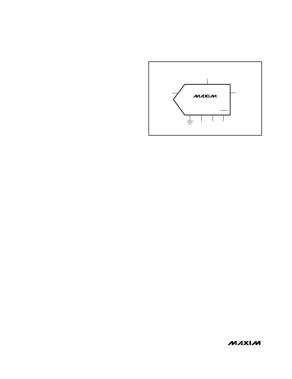
Voltage Mode (MAX551)
The MAX551 can be conveniently used in voltage
mode, single-supply operation with OUT biased at any
voltage between GND and V
DD
. OUT must not be
allowed to go 0.3V lower than GND or 0.3V higher than
V
DD
. Otherwise, internal diodes will turn on, causing a
high current flow that could damage the device.
+3V/+5V, 12-Bit, Serial, Multiplying DACs
in 10-Pin µMAX Package
10
______________________________________________________________________________________
+5V
REF
GND
DIN
OUT
V
DD
SCLK
LOAD
REFERENCE
VOLTAGE
V
OUT
MAX551
Figure 5. Single-Supply, Voltage Mode Operation