Table 8. control register (address: 0x2) – Rainbow Electronics MAX1471 User Manual
Page 23
MAX1471
315MHz/434MHz Low-Power, 3V/5V
ASK/FSK Superheterodyne Receiver
______________________________________________________________________________________
23
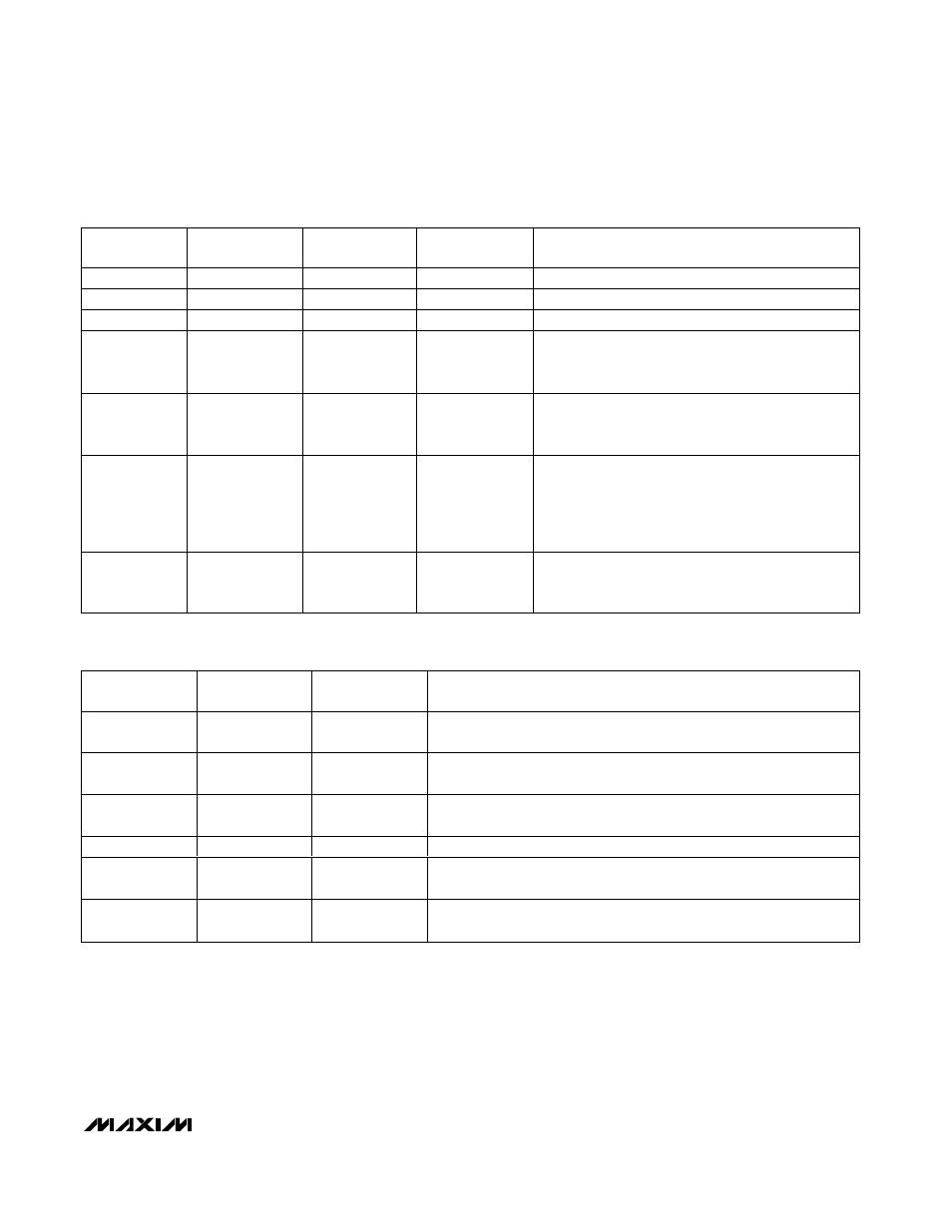
Table 8. Control Register (Address: 0x2)
BIT ID
BIT NAME
BIT LOCATION
(0 = LSB)
POWER-UP
STATE
FUNCTION
X
None
7
Don’t care
Don’t care.
AGCLOCK
AGC lock
6
0
Locks the LNA gain in its present state.
X
None
5, 4
Don’t care.
FSKTRK_EN
FSK peak
detector track
enable
3
0
Enables the tracking mode of the FSK peak detectors
when FSKTRK_EN = 1. (See the Peak Detectors
section.)
ASKTRK_EN
ASK peak
detector track
enable
2
0
Enables the tracking mode of the ASK peak detectors
when ASKTRK_EN = 1.
(See the Peak Detectors section.)
POL_CAL_EN
Polling timer
calibration enable
1
0
POL_CAL_EN = 1 starts the polling timer calibration.
Calibration of the polling timer is needed when using
the MAX1471 in discontinous receive mode.
POL_CAL_EN resets when calibration completes
properly. (See the Calibration section.)
FSK_CAL_EN
FSK calibration
enable
0
0
FSK_CAL_EN starts the FSK receiver calibration.
FSK_CAL_EN resets when calibration completes
properly. (See the Calibration section.)
Table 9. Status Register (Read Only) (Address: 0x9)
BIT ID
BIT NAME
BIT LOCATION
(0 = LSB)
FUNCTION
LOCKDET
Lock detect
7
0 = Internal PLL is not locked so the MAX1471 will not receive data.
1 = Internal PLL is locked.
AGCST
AGC state
6
0 = LNA in low-gain state.
1 = LNA in high-gain state.
CLKALIVE
Clock/crystal
alive
5
0 = No valid clock signal seen at the crystal inputs.
1 = Valid clock at crystal inputs.
X
None
4, 3, 2
Don’t care.
POL_CAL_DONE
Polling timer
calibration done
1
0 = Polling timer calibraton in progress or not completed.
1 = Polling timer calibration is complete.
FSK_CAL_DONE
FSK calibration
done
0
0 = FSK calibration in progress or not completed.
1 = FSK calibration is compete.