Absolute maximum ratings, Dc electrical characteristics – Rainbow Electronics MAX1471 User Manual
Page 2
MAX1471
315MHz/434MHz Low-Power, 3V/5V
ASK/FSK Superheterodyne Receiver
2
_______________________________________________________________________________________
ABSOLUTE MAXIMUM RATINGS
Stresses beyond those listed under “Absolute Maximum Ratings” may cause permanent damage to the device. These are stress ratings only, and functional
operation of the device at these or any other conditions beyond those indicated in the operational sections of the specifications is not implied. Exposure to
absolute maximum rating conditions for extended periods may affect device reliability.
High-Voltage Supply, HV
IN
to DGND .......................-0.3V, +6.0V
Low-Voltage Supply, AV
DD
and DV
DD
to AGND .....-0.3V, +4.0V
SCLK, DIO,
CS, ADATA,
FDATA ....................................(DGND - 0.3V) to (HV
IN
+ 0.3V)
All Other Pins.............................(AGND - 0.3V) to (AV
DD
+ 0.3V)
Continuous Power Dissipation (T
A
= +70°C)
32-Pin Thin QFN (derate 21.3mW/°C above +70°C) ...1702mW
Operating Temperature Range .........................-40°C to +125°C
Junction Temperature ......................................................+150°C
Storage Temperature Range .............................-65°C to +150°C
Lead Temperature (soldering, 10s) ................................ +300°C
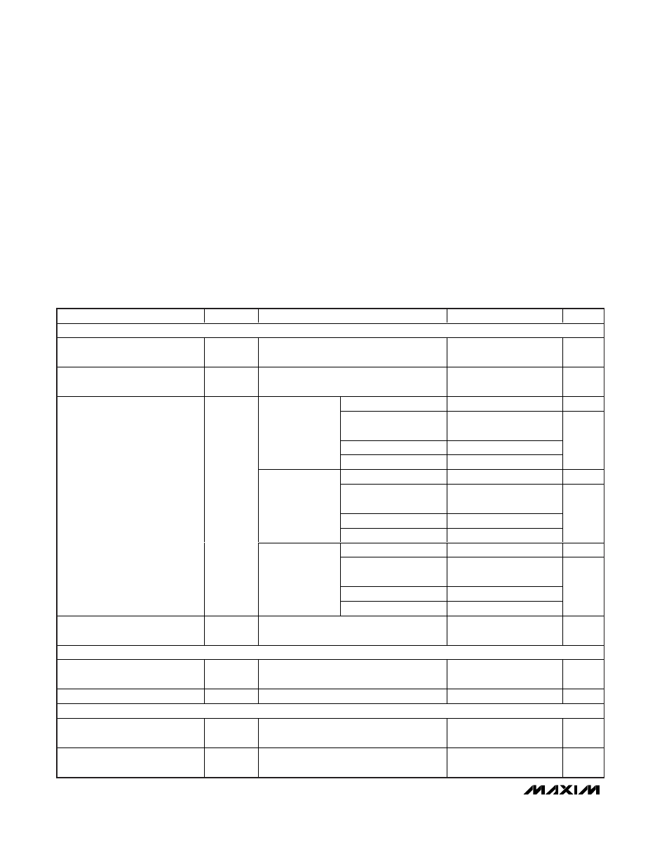
DC ELECTRICAL CHARACTERISTICS
(Typical Application Circuit, AV
DD
= DV
DD
= HV
IN
= +2.4V to +3.6V, f
RF
= 300MHz to 450MHz, T
A
= -40°C to +125°C, unless otherwise
noted. Typical values are at AV
DD
= DV
DD
= HV
IN
= +3.0V, f
RF
= 434 MHz, T
A
= +25°C, unless otherwise noted.) (Note 1)
PARAMETER
SYMBOL
CONDITIONS
MIN
TYP
MAX
UNITS
GENERAL CHARACTERISTICS
Supply Voltage (5V)
HV
IN
AV
DD
and DV
DD
unconnected from HV
IN
,
but connected together
4.5
5.0
5.5
V
Supply Voltage (3V)
V
DD
HV
IN
, AV
DD
, and DV
DD
connected to power
supply
2.4
3.0
3.6
V
Operating
7.0
8.4
mA
Polling duty cycle: 10%
duty cycle
705
855
DRX mode OFF current
5.0
14.2
T
A
< +85°C
Deep-sleep current
1.1
7.1
µA
Operating
8.5
mA
Polling duty cycle: 10%
duty cycle
865
DRX mode OFF current
15.5
T
A
< +105°C
(Note 2)
Deep-sleep current
13.4
µA
Operating
8.6
mA
Polling duty cycle: 10%
duty cycle
900
DRX mode OFF current
44.1
Supply Current
I
DD
T
A
< +125°C
(Note 2)
Deep-sleep current
36.4
µA
Startup Time
t
ON
Time for final signal detection, does not
include baseband filter settling (Note 2)
200
250
µs
DIGITAL OUTPUTS (DIO, ADATA, FDATA)
Output High Voltage
V
OH
I
SOURCE
= 250µA (Note 2)
HV
IN
-
0.15
V
Output Low Voltage
V
OL
I
SINK
= 250µA (Note 2)
0.15
V
DIGITAL INPUTS (
CS, DIO, SCLK)
Input High Threshold
V
IH
0.9 x
HV
IN
V
Input Low Threshold
V
IL
.
0.1 x
HV
IN
V