Detailed description, Pin description (continued) – Rainbow Electronics MAX1821 User Manual
Page 9

MAX1820/MAX1821
WCDMA Cellular Phone 600mA
Buck Regulators
_______________________________________________________________________________________
9
_______________Detailed Description
The MAX1820/MAX1821 PWM step-down DC-DC con-
verters are optimized for low-voltage, battery-powered
applications where high efficiency and small size are
priorities. The MAX1821 is a general-purpose device
that uses external feedback resistors to set the output
voltage from 1.25V to V
BATT
, and the MAX1820 is
specifically intended to power a linear PA in WCDMA
handsets. An analog control signal dynamically adjusts
the MAX1820’s output voltage from 0.4V to 3.4V with a
settling time <30µs.
The MAX1820/MAX1821 operate at a high 1MHz
switching frequency that reduces external component
size. Each device includes an internal synchronous rec-
tifier that provides for high efficiency and eliminates the
need for an external Schottky diode. The normal operat-
ing mode uses constant-frequency PWM switching at
medium and heavy loads, and automatically pulse
skips at light loads to reduce supply current and extend
battery life. An additional forced PWM mode (with
optional external synchronization) switches at a con-
stant frequency, regardless of load, to provide a well-
controlled spectrum in noise-sensitive applications.
Battery life is maximized by low-dropout operation at
100% duty-cycle and a 0.1µA (typ) logic-controlled
shutdown mode.
PWM Control
The MAX1820/MAX1821 use a slope-compensated,
current-mode PWM controller capable of achieving
100% duty cycle. The current-mode control design is
capable of minimum duty cycles of less than 10%,
ensuring a constant switching frequency with outputs
as low as 0.4V when powered from a single lithium-ion
(Li+) cell. Current-mode feedback provides stable
switching and cycle-by-cycle current limiting for superi-
or load and line response and protection of the internal
MOSFET and synchronous rectifier. The output voltage
is regulated by switching at a constant frequency and
then modulating the power transferred to the load dur-
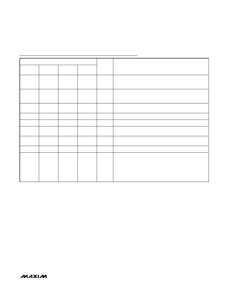
Pin Description (continued)
PIN
MAX1820
UCSP
MAX1820
µMAX
MAX1821
UCSP
MAX1821
µMAX
NAME
FUNCTION
—
—
A3
3
FB
Output Feedback Sense Input. To set the output voltage,
connect FB to the center of an external resistive divider between
the output and GND. FB voltage regulates to 1.25V.
A4
4
—
—
REF
External Reference Input. Connect REF to the output of a D/A
converter for dynamic adjustment of the output voltage. REF-to-
OUT gain is 1.76.
—
—
A4
4
REF
Internal Reference Bypass. Connect a 0.047µF capacitor from
REF to GND.
B4
5
B4
5
GND
Ground
C4
6
C4
6
PGND
Power Ground
C3
7
C3
7
LX
Inductor Connection. LX connects to the drains of the internal
power MOSFETs. LX is high impedance in shutdown mode.
C2
8
C2
8
BATT
Supply Voltage Input. Connect BATT to a 2.6V to 5.5V source.
Bypass BATT to PGND with a low-ESR 10µF capacitor.
C1
9
C1
9
SHDN
Active-Low, Shutdown Control Input
B1
10
B1
10
SYNC
Clock Synchronization Input. Drive SYNC with a 13MHz
(MAX1820X, MAX1821X) or 19.8MHz (MAX1820Y) AC-coupled
sine-wave input to synchronize power switching at 1MHz.
MAX1820Z and MAX1821 do not have SYNC capability.
Connect SYNC to GND to use the internally generated,
free-running 1MHz clock. MAX1820Z and MAX1821 SYNC pin
must be connected to GND.
