Rainbow Electronics MAX1821 User Manual
Page 10
MAX1820/MAX1821
WCDMA Cellular Phone 600mA
Buck Regulators
10
______________________________________________________________________________________
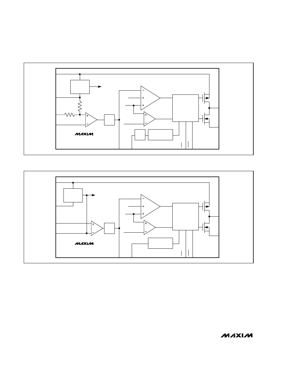
ing each cycle, using the PWM comparator. The power
transferred to the load is adjusted by changes in the
inductor peak current limit during the first half of each
cycle, based on the output error voltage.
A new cycle begins at each falling edge of the internal
oscillator. The controller turns on the P-channel MOS-
FET to increase the inductor current, and the slope
compensation block initiates a new reference current
ramp that is summed with the internal P-channel MOS-
FET current (Figures 1 and 2).
The second half of the cycle begins when the reference
ramp is greater than the error voltage. The P-channel
MOSFET is turned off, the synchronous rectifier is
turned on, and inductor current continues to flow to the
output capacitor. The output capacitor stores charge
when the current is high and releases it when the
inductor current is low, smoothing the voltage across
VOLTAGE
REFERENCE
PWM CONTROL
AND
SKIP LOGIC
ERROR SIGNAL
SLOPE COMP
CURRENT SENSE
SKIP THRESHOLD
TRANSIMPEDANCE
ERROR AMP
MAX1820
SKIP
COMPARATOR
PWM
COMPARATOR
LX
PGND
÷13 OR
÷18
1.25V
TO
IC BIAS
0.45V TO 2.15V
1MHz
OSCILLATOR
CLAMP
COMP
SYNC
SKIP
SHDN
GND
BATT
OUT
REF
Figure 1. MAX1820 Simplified Functional Diagram (No SYNC for MAX1820Z)
VOLTAGE
REFERENCE
PWM CONTROL
AND
SKIP LOGIC
ERROR SIGNAL
SLOPE COMP
CURRENT SENSE
SKIP THRESHOLD
TRANSIMPEDANCE
ERROR AMP
MAX1821
SKIP
COMPARATOR
PWM
COMPARATOR
LX
PGND
1.25V
TO
IC BIAS
0.45V TO 2.15V
1MHz
OSCILLATOR
CLAMP
COMP
SYNC
SKIP
SHDN
GND
BATT
OUT
REF
Figure 2. MAX1821 Simplified Functional Diagram (No SYNC for MAX1821)