Pin description, Typical operating characteristics (continued) – Rainbow Electronics MAX1821 User Manual
Page 8
MAX1820/MAX1821
WCDMA Cellular Phone 600mA
Buck Regulators
8
_______________________________________________________________________________________
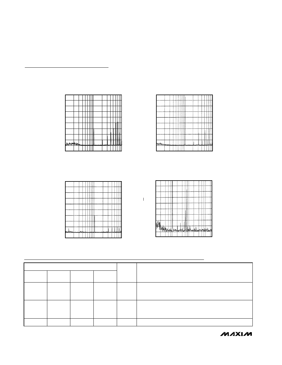
0.1
1
10
OUTPUT SWITCHING HARMONICS
vs. FREQUENCY
(V
IN
= 3.8V, V
OUT
= 3.4V, I
LOAD
= 600mA)
MAX1820/21 toc19
FREQUENCY (MHz)
HARMONICS (mV
RMS
)
1.6
1.2
0.8
0.4
0
0.1
1
10
OUTPUT SWITCHING HARMONICS
vs. FREQUENCY
(V
IN
= 3.8V, V
OUT
= 1.8V, I
LOAD
= 300mA)
MAX1820/21 toc20
FREQUENCY (MHz)
HARMONICS (mV
RMS
)
0
0.8
0.4
1.6
1.2
Pin Description
PIN
MAX1820
UCSP
MAX1820
µMAX
MAX1821
UCSP
MAX1821
µMAX
NAME
FUNCTION
A1
1
A1
1
SKIP
PWM/Skip-Mode Input. Drive with logic 0 to use PWM at medium
and heavy loads and pulse skipping at light loads. Drive with
logic 1 to force PWM at all loads.
A2
2
A2
2
COMP
Compensation. Typically, connect an 82k
Ω (for MAX1821) or
43k
Ω (for MAX1820) series resistor and 330pF capacitor from
this pin to GND to stabilize the regulator.
A3
3
—
—
OUT
Output Voltage Sense Input. Connect OUT directly to the output.
0.1
1
10
OUTPUT SWITCHING HARMONICS
vs. FREQUENCY
(V
IN
= 4.2V, V
OUT
= 0.4V, I
LOAD
= 30mA)
MAX1820/21 toc21
FREQUENCY (MHz)
HARMONICS (mV
RMS
)
0
0.8
0.4
1.6
1.2
FREQUENCY (MHz)
OUTPUT NOISE (V
IN
= 3.6V,
V
OUT
= 1.8V, I
OUT
= 300mA)
4.0
3.0
1.0
2.0
MAX1820/21 toc22
0
0.1
1
10
100
250
NOISE (
µ
V/
√
Hz)
Typical Operating Characteristics (continued)
(T
A
= +25°C, unless otherwise noted.)