Rainbow Electronics MAX1821 User Manual
Page 11

MAX1820/MAX1821
WCDMA Cellular Phone 600mA
Buck Regulators
______________________________________________________________________________________
11
the load. The duty cycle of a buck step-down converter
is ideally a ratio of the output voltage to input voltage in
steady-state condition.
The MAX1820/MAX1821 have internal switch current
limits of 1.2A (typ). If I
LX
exceeds this maximum, the
high-side FET turns off and the synchronous rectifier
turns on. This lowers the duty cycle and causes the out-
put voltage to droop as long as the load current
remains excessive. There is also a synchronous rectifier
current limit of -0.85A when the device is operating in
forced PWM mode (see the Forced PWM Operation sec-
tion). If the negative current limit is exceeded, the syn-
chronus rectifier is turned off, and the inductor current
continues to flow through its body diode until the begin-
ning of the next cycle or the inductor current drops to
zero. This means there is a limit on how much current
the device is allowed to shuttle in response to output
power reduction.
Normal Mode Operation
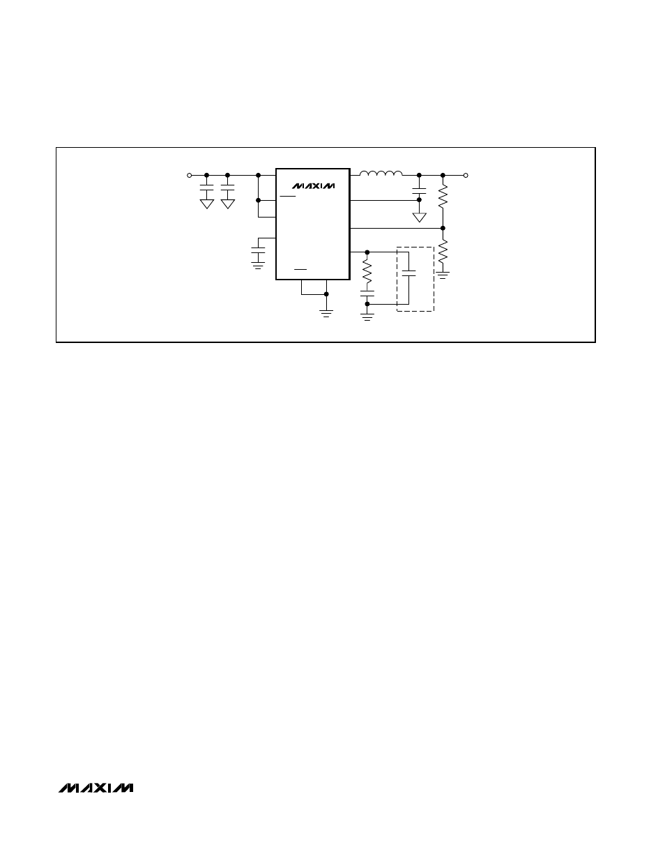
Connecting SKIP to GND enables MAX1820/MAX1821
normal operation (Figure 3). This allows automatic PWM
control at medium and heavy loads and skip mode at
light loads to improve efficiency and reduce quiescent
current to 180µA. Operating in normal mode also allows
the MAX1820/MAX1821 to pulse skip when the peak
inductor current drops below 130mA, corresponding to
a load current of approximately 65mA.
During skip operation, the MAX1820/MAX1821 switch
only as needed to service the load, reducing the
switching frequency and associated losses in the inter-
nal switch, the synchronous rectifier, and the external
inductor.
There are three steady-state operating conditions for
the MAX1820/MAX1821 in normal mode. The device
performs in continuous conduction for heavy loads in a
manner identical to forced PWM mode. The inductor
current becomes discontinuous at medium loads,
requiring the synchronous rectifier to be turned off
before the end of a cycle as the inductor current reach-
es zero. The device enters into skip mode when the
converter output voltage exceeds its regulation limit
before the inductor current reaches its skip thres-
hold level.
During skip mode, a switching cycle initiates when the
output voltage has dropped out of regulation. The P-
channel MOSFET switch turns on and conducts current
to the output-filter capacitor and load until the inductor
current reaches the skip peak current limit. Then the
main switch turns off, and the magnetic field in the
inductor collapses, while current flows through the syn-
chronous rectifier to the output filter capacitor and the
load. The synchronous rectifier is turned off when the
inductor current reaches zero. The MAX1820/ MAX1821
wait until the skip comparator senses a low output volt-
age again.
Forced PWM Operation
Connect SKIP to BATT for forced PWM operation.
Forced PWM operation is desirable in sensitive RF and
data-acquisition applications to ensure that switching
harmonics do not interfere with sensitive IF and data-
sampling frequencies. A minimum load is not required
during forced PWM operation since the synchronous
rectifier passes reverse-inductor current as needed to
allow constant-frequency operation with no load.
BATT
LX
PGND
FB
COMP
SYNC
REF
SKIP
GND
SHDN
R1
6k
Ω
R
C
82k
Ω
C1
330pF
R2
30k
Ω
4.7
µH
4.7
µF
0.047
µF
V
IN
= 2.6V TO 5.5V
* CAN BE OMITTED IF CERAMIC OUTPUT CAPACITOR IS USED.
V
OUT
= 1.5V
C2*
1pF
MAX1821
10
µF
0.1
µF
Figure 3. Standard Operating Circuit
