Grounding, bypassing, and board layout – Rainbow Electronics MAX1181 User Manual
Page 14
MAX1181
Dual 10-Bit, 80Msps, +3V, Low-Power ADC with
Internal Reference and Parallel Outputs
14
______________________________________________________________________________________
The 22pF C
IN
capacitor acts as a small bypassing
capacitor.
Using Transformer Coupling
An RF transformer (Figure 6) provides an excellent
solution to convert a single-ended source signal to a
fully-differential signal, required by the MAX1181 for
optimum performance. Connecting the center tap of the
transformer to COM provides a V
DD
/2 DC level shift to
the input. Although a 1:1 transformer is shown, a step-
up transformer may be selected to reduce the drive
requirements. A reduced signal swing from the input
driver, such as an op amp, may also improve the over-
all distortion.
In general, the MAX1181 provides better SFDR and
THD with fully-differential input signals, than a single-
ended drive, especially for high input frequencies. In
differential input mode, even-order harmonics are lower
as both inputs (INA+, INA- and/or INB+, INB-) are bal-
anced, and each of the ADC inputs only require half the
signal swing compared to single-ended mode.
Single-Ended AC-Coupled Input Signal
Figure 7 shows an AC-coupled, single-ended applica-
tion. Amplifiers, like the MAX4108, provide high-speed,
high bandwidth, low-noise, and low distortion to main-
tain the integrity of the input signal.
Typical QAM Demodulation Application
The most frequently used modulation technique for dig-
ital communications application is the Quadrature
Amplitude Modulation (QAM). QAMs are typically found
in spread-spectrum based systems. A QAM signal rep-
resents a carrier frequency modulated in both ampli-
tude and phase. At the transmitter, modulating the
baseband signal with quadrature outputs, a local oscil-
lator followed by subsequent up-conversion can gener-
ate the QAM signal. The result is an in-phase (I) and a
quadrature (Q) carrier component, where the Q compo-
nent is 90 degrees phase-shifted with respect to the in-
phase component. At the receiver, the QAM signal is
divided down into its I and Q components, essentially
representing the modulation process reversed. Figure 8
displays the demodulation process performed in the
analog domain, using the dual-matched, +3V, 10-bit
ADCs, MAX1181 and the MAX2451 quadrature demod-
ulators, to recover and digitize the I and Q baseband
signals. Before being digitized by the MAX1181, the
mixed-down signal components may be filtered by
matched analog filters, such as Nyquist or pulse-shap-
ing filters which remove any unwanted images from the
mixing process, enhances the overall signal-to-noise
(SNR) performance, and minimizes intersymbol interfer-
ence.
Grounding, Bypassing,
and Board Layout
The MAX1181 requires high-speed board layout design
techniques. Locate all bypass capacitors as close to
the device as possible, preferably on the same side as
the ADC, using surface-mount devices for minimum
inductance. Bypass V
DD
, REFP, REFN, and COM with
two parallel 0.1µF ceramic capacitors and a 2.2µF
bipolar capacitor to GND. Follow the same rules to
bypass the digital supply (OV
DD
) to OGND. Multilayer
boards with separate ground and power planes, pro-
duce the highest level of signal integrity. Consider the
use of a split ground plane arranged to match the phys-
ical location of the analog ground (GND) and the digital
output driver ground (OGND) on the ADCs package.
The two ground planes should be joined at a single
point, such that the noisy digital ground currents do not
interfere with the analog ground plane. The ideal loca-
tion of this connection can be determined experimental-
ly at a point along the gap between the two ground
planes, which produces optimum results. Make this
connection with a low-value, surface-mount resistor (1
Ω
to 5
Ω), a ferrite bead, or a direct short. Alternatively, all
ground pins could share the same ground plane, if the
ground plane is sufficiently isolated from any noisy, dig-
ital systems ground plane (e.g., downstream output
buffer or DSP ground plane). Route high-speed digital
signal traces away from the sensitive analog traces of
either channel. Make sure to isolate the analog input
lines to each respective converter to minimize channel-
to-channel crosstalk. Keep all signal lines short and
free of 90 degree turns.
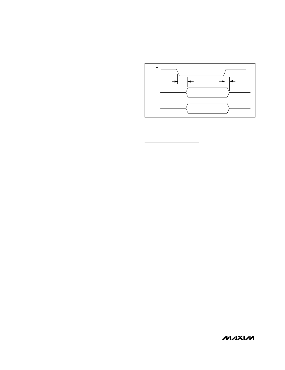
OUTPUT
D9A–D0A
OE
t
DISABLE
t
ENABLE
HIGH-Z
HIGH-Z
VALID DATA
OUTPUT
D9B–D0B
HIGH-Z
HIGH-Z
VALID DATA
Figure 4. Output Timing Diagram