Applications information – Rainbow Electronics MAX1181 User Manual
Page 13
of the MAX1181 small-series resistors (e.g., 100
Ω), add
to the digital output paths, close to the MAX1181.
Figure 4 displays the timing relationship between out-
put enable and data output valid, as well as power-
down/wake-up and data output valid.
Power-Down (PD) and Sleep
(SLEEP) Modes
The MAX1181 offers two power-save modes; sleep and
full power-down mode. In sleep mode (SLEEP = 1),
only the reference bias circuit is active (both ADCs are
disabled) and current consumption is reduced to
2.8mA.
To enter full power-down mode, pull PD high. With OE
simultaneously low, all outputs are latched at the last
value prior to the power-down. Pulling OE high, forces
the digital outputs into a high-impedance state.
Applications Information
Figure 5 depicts a typical application circuit containing
two single-ended to differential converters. The internal
reference provides a V
DD
/2 output voltage for level-
shifting purposes. The input is buffered and then split
to a voltage follower and inverter. One lowpass filter per
ADC suppresses some of the wideband noise associat-
ed with high-speed operational amplifiers. The user
may select the R
ISO
and C
IN
values to optimize the fil-
ter performance to suit a particular application. For the
application in Figure 5, a R
ISO
of 50
Ω is placed before
the capacitive load to prevent ringing and oscillation.
MAX1181
Dual 10-Bit, 80Msps, +3V, Low-Power ADC with
Internal Reference and Parallel Outputs
______________________________________________________________________________________________________
13
DIFFERENTIAL INPUT
VOLTAGE*
DIFFERENTIAL INPUT
STRAIGHT OFFSET
BINARY
T/B = 0
TWO’S COMPLEMENT
T/B = 1
V
REF
✕
511/512
+FULL SCALE - 1LSB
11 1111 1111
01 1111 1111
V
REF
✕
1/512
+ 1 LSB
10 0000 0001
00 0000 0001
0
Bipolar Zero
10 0000 0000
00 0000 0000
-V
REF
✕
1/512
- 1 LSB
01 1111 1111
11 1111 1111
-V
REF
✕
511/512
- FULL SCALE + 1 LSB
00 0000 0001
10 0000 0001
-V
REF
✕
512/512
- FULL SCALE
00 0000 0000
10 0000 0000
Table 1. MAX1181 Output Codes For Differential Inputs
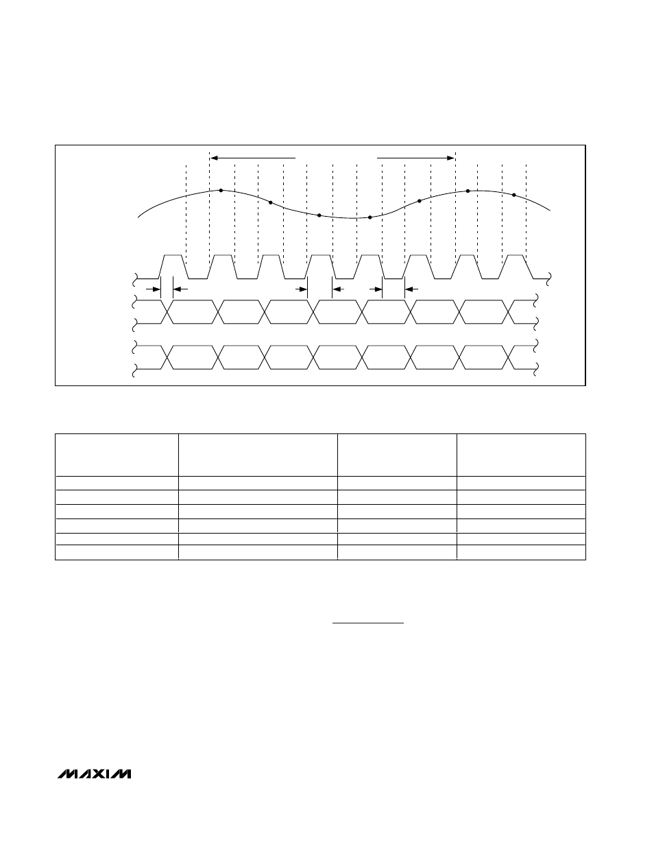
N - 6
N
N - 5
N + 1
N - 4
N + 2
N - 3
N + 3
N - 2
N + 4
N - 1
N + 5
N
N + 6
N + 1
5 CLOCK-CYCLE LATENCY
ANALOG INPUT
CLOCK INPUT
DATA OUTPUT
D9A–D0A
t
D0
t
CH
t
CL
N - 6
N - 5
N - 4
N - 3
N - 2
N - 1
N
N + 1
DATA OUTPUT
D9B–D0B
Figure 3. System Timing Diagram
*V
REF
= V
REFP
- V
REFN