Max1181 – Rainbow Electronics MAX1181 User Manual
Page 12
MAX1181
five clock cycle latency between any particular sample
and its corresponding output data. The output coding
can be chosen to be either straight offset binary or two’s
complement (Table 1) controlled by a single pin (T/B).
Pull T/B low to select offset binary and high to activate
two’s complement output coding. The capacitive load
on the digital outputs D0A–D9A and D0B–D9B should
be kept as low as possible (<15pF), to avoid large digi-
tal currents that could feed back into the analog portion
of the MAX1181, thereby degrading its dynamic perfor-
mance. Using buffers on the digital outputs of the ADCs
can further isolate the digital outputs from heavy capaci-
tive loads. To further improve the dynamic performance
Dual 10-Bit, 80Msps, +3V, Low-Power ADC with
Internal Reference and Parallel Outputs
12
______________________________________________________________________________________
S3b
S3a
COM
S5b
S5a
INB+
INB-
S1
OUT
OUT
C2a
C2b
S4c
S4a
S4b
C1b
C1a
INTERNAL
BIAS
INTERNAL
BIAS
COM
HOLD
HOLD
CLK
INTERNAL
NONOVERLAPPING
CLOCK SIGNALS
TRACK
TRACK
S2a
S2b
S3b
S3a
COM
S5b
S5a
INA+
INA-
S1
OUT
OUT
C2a
C2b
S4c
S4a
S4b
C1b
C1a
INTERNAL
BIAS
INTERNAL
BIAS
COM
S2a
S2b
MAX1181
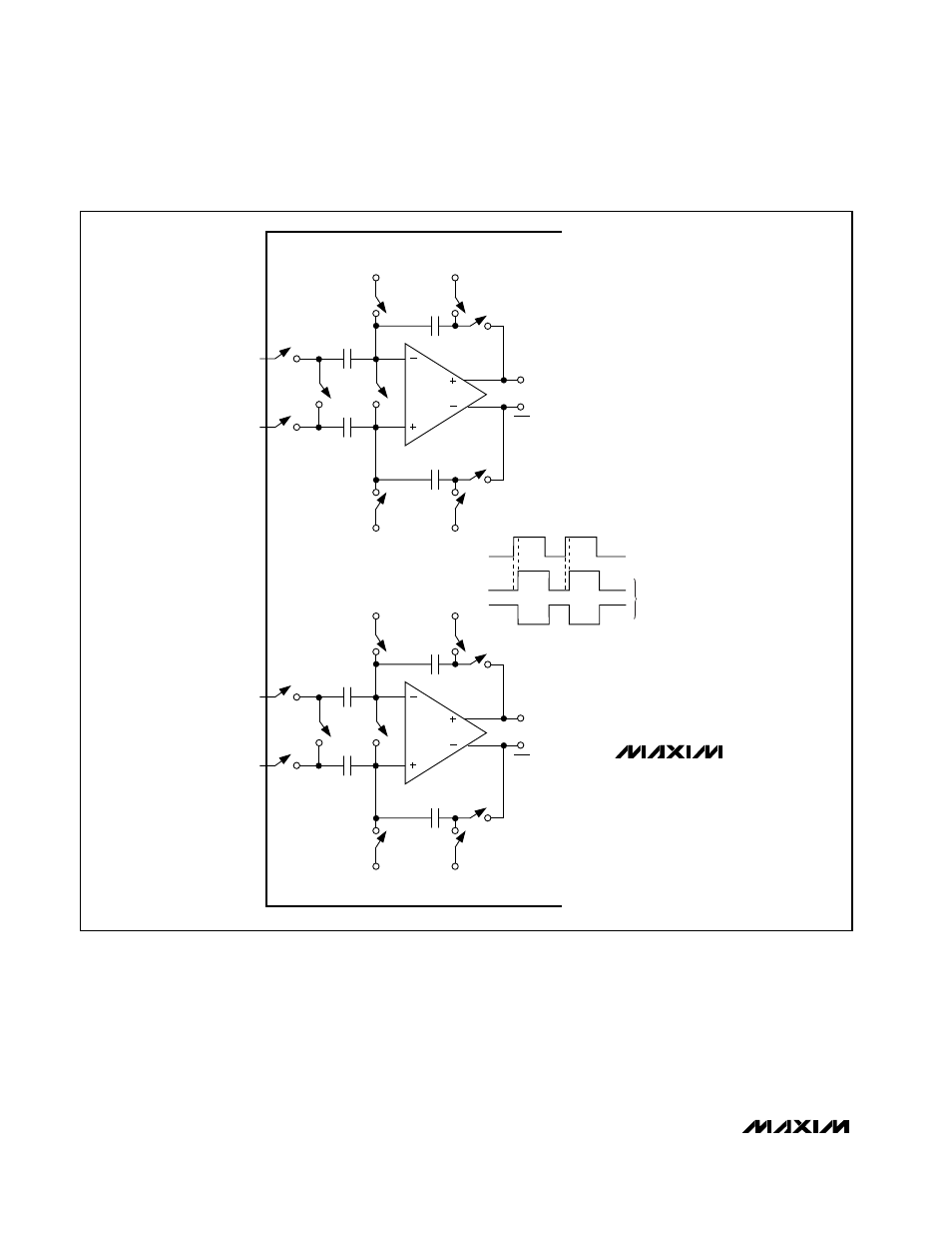
Figure 2. MAX1181 T/H Amplifiers