Pin description – Rainbow Electronics MAX3673 User Manual
Page 8
MAX3673
Low-Jitter Frequency Synthesizer
with Selectable Input Reference
8
_______________________________________________________________________________________
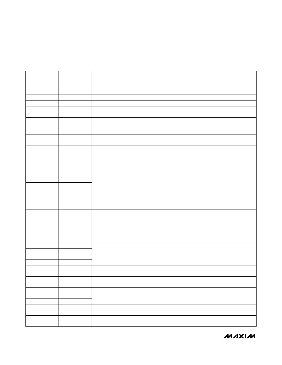
Pin Description
PIN
NAME
FUNCTION
1
IN0FAIL
REFCLK0 Failure Indicator, LVCMOS/LVTTL Output. Low indicates REFCLK0 fails the clock
qualification. Once a failed clock is detected, the indicator status is latched and updated
every 128 PFD cycles (~ 2μs).
2
RSVD1
Reserved. Leave pin open.
3
RSVD2
Reserved. Connect to GND.
4 REFCLK0
5
REFCLK0
Reference Clock Input 0, Differential LVPECL
6
DM
Four-Level Control Input for Reference Clock Input Divider. See Table 1.
7, 22, 30, 41,
49, 52
V
CC
Power Supply. Connect to +3.3V.
8, 14, 23, 29,
42, 48, 53
GND Supply
Ground
9
MR
Master Reset, LVCMOS/LVTTL Input. Connect this pin high or leave open for normal
operation. Has internal 90k
pullup to V
CC
. Connect low to reset the device. A reset is not
required at power-up. If the output divider settings are changed on the fly, a reset is
required to phase align the outputs. This input has a 100ns minimum pulse width and is
asynchronous to the reference clock. While in reset, all clock outputs are held to logic-
low. See Table 6.
10 REFCLK1
11
REFCLK1
Reference Clock Input 1, Differential LVPECL
12 SEL_CLK
Reference Clock Select, LVCMOS/LVTTL Input. Connect low or leave open to select REFCLK0
as the reference clock. Has internal 90k
pulldown to GND. Connect high to select REFCLK1
as the reference clock.
13
VCC_VCO
Power Supply for VCO. Connect to +3.3V.
15
CPLL
Connection for PLL Filter Capacitor. Connect a 0.1μF capacitor between this pin and GND.
16 CREG
Connection for VCO Regulator Capacitor. Connect a 0.22μF capacitor between this pin and
GND.
17 FB_SEL
External Feedback Select, LVCMOS/LVTTL Input. Connect high to select external feedback
for zero-delay buffer configuration. Connect low or leave open for internal feedback. Has
internal 90k
pulldown to GND.
18 FB_IN
19
FB_IN
External Feedback Clock Input, Differential LVPECL. Used for zero-delay buffer
configuration.
20
OUTB0
21 OUTB0
Clock Output B0, Differential LVPECL
24
OUTB1
25 OUTB1
Clock Output B1, Differential LVPECL
26
OUTB2
27 OUTB2
Clock Output B2, Differential LVPECL
28
DB
Four-Level Control Input for B-Group Output Divider. See Table 3.
31
OUTB3
32 OUTB3
Clock Output B3, Differential LVPECL
33
OUTB4
34 OUTB4
Clock Output B4, Differential LVPECL
35
OUTB_EN
Three-Level Control Input for B-Group Output Enable. See Table 5.
36
OUTA_EN
Three-Level Control Input for A-Group Output Enable. See Table 4.