Table 4. outa[3:0] enable control, Table 5. outb[4:0] enable control – Rainbow Electronics MAX3673 User Manual
Page 11
MAX3673
Low-Jitter Frequency Synthesizer
with Selectable Input Reference
______________________________________________________________________________________
11
PLL Out-of-Lock Condition
If the frequency difference between the reference clock
input and the VCO at the PFD input becomes within
500ppm, the PLL is considered to be in lock (LOCK =
0). When the frequency difference between the refer-
ence clock input and the VCO at the PFD input
becomes greater than 800ppm, the PLL is considered
out-of-lock. It should be noted that the LOCK indicator
is not part of the frequency qualification used for the
INxFAIL indicators.
Input and Output Frequencies
The MAX3673 input and output dividers are configured
using four-level control inputs DM, DA, and DB. Each
divider is independent and can have a unique setting.
The input connection and associated frequencies are
listed in Tables 1, 2, and 3.
Output-Enable Controls
Each output group (A and B) has a three-level control
input OUTA_EN and OUTB_EN. See Tables 4 and 5 for
configuration settings. When clock outputs are dis-
abled, they are high impedance. Unused enabled out-
puts should be left open.
Power-On-Reset (POR)
At power-on, an internal signal is generated to hold the
MAX3673 in a reset state. This internal reset time is
about 20µs after V
CC
reaches 3.0V (Figure 2). During
the POR time, the outputs are held to logic-low (OUTxx
= low and OUTxx = high). See Table 6 for output signal
status during POR. After this internal reset time, the PLL
starts to lock to the reference clock selected by
SEL_CLK.
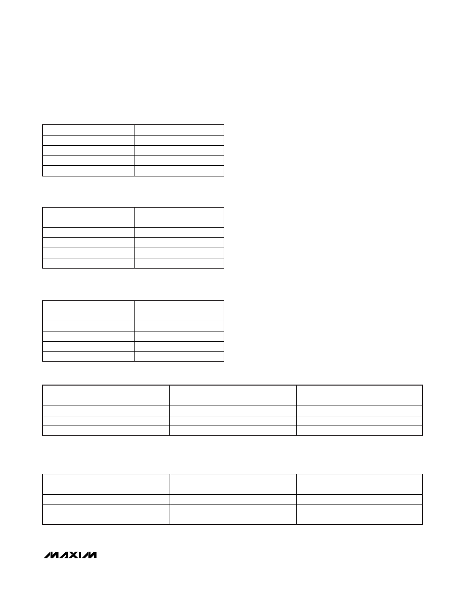
Table 1. Divider M Configuration for Input
Frequencies
CONNECTION FROM DM PIN
INPUT FREQUENCY (MHz)
GND 61.44
V
CC
122.88
Open 245.76
10k
to GND
307.2
Table 2. Divider A Configuration for
A-Group Output Frequencies
CONNECTION FROM DA PIN
OUTPUT FREQUENCY AT
OUTA[3:0] (MHz)
GND 61.44
V
CC
122.88
Open 153.6
10k
to GND
307.2
Table 3. Divider B Configuration for
B-Group Output Frequencies
CONNECTION FROM DB PIN
OUTPUT FREQUENCY AT
OUTB[4:0] (MHz)
GND 61.44
V
CC
122.88
Open 245.76
10k
to GND
307.2
Table 4. OUTA[3:0] Enable Control
CONNECTION FROM
OUTA_EN PIN
A-GROUP OUTPUT ENABLED
A-GROUP OUTPUT DISABLED TO HIGH
IMPEDANCE
GND
OUTA0, OUTA1, OUTA2, OUTA3
—
V
CC
*
—
OUTA0, OUTA1, OUTA2, OUTA3
Open
OUTA0, OUTA1
OUTA2, OUTA3
Table 5. OUTB[4:0] Enable Control
CONNECTION FROM
OUTB_EN PIN
B-GROUP OUTPUT ENABLED
B-GROUP OUTPUT DISABLED TO HIGH
IMPEDANCE
GND
OUTB0, OUTB1, OUTB2, OUTB3, OUTB4
—
V
CC
*
OUTB0
OUTB1, OUTB2, OUTB3, OUTB4
Open
OUTB0, OUTB1, OUTB2
OUTB3, OUTB4
*Connecting both OUTA_EN and OUTB_EN to V
CC
enables a factory test mode and forces all indicators to GND. This is not a valid
mode of operation.
*Connecting both OUTA_EN and OUTB_EN to V
CC
enables a factory test mode and forces all indicators to GND. This is not a valid
mode of operation.