Pin description (continued) – Rainbow Electronics MAX1121 User Manual
Page 9
MAX1121
1.8V, 8-Bit, 250Msps Analog-to-Digital Converter
with LVDS Outputs for Wideband Applications
_______________________________________________________________________________________
9
Pin Description (continued)
PIN
NAME
FUNCTION
50
D4N
Complementary Output Bit 4
51
D4P
True Output Bit 4
52
D5N
Complementary Output Bit 5
53
D5P
True Output Bit 5
54
D6N
Complementary Output Bit 6
55
D6P
True Output Bit 6
56
D7N
Complementary Output Bit 7
57
D7P
True Output Bit 7
58
ORN
Complementary Output for Out-of-Range Control Bit. If an out-of-range condition is detected,
bit ORN flags this condition by transitioning low.
59
ORP
True Output for Out-of-Range Control Bit. If an out-of-range condition is detected, bit ORP
flags this condition by transitioning high.
68
T/B
Two’s Complement or Binary Output Format Selection. This LVCMOS-compatible input
controls the digital output format of the MAX1121.
T/B has an internal pulldown resistor.
T/B = 0: Two’s complement output format
T/B = 1: Binary output format
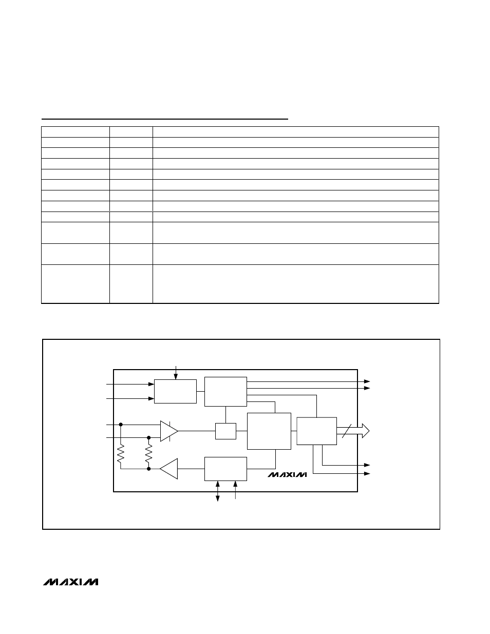
CLOCK-
DIVIDER
CONTROL
CLOCK
MANAGEMENT
T/H
8-BIT PIPELINE
QUANTIZER CORE
REFERENCE
LVDS
DATA PORT
8
COMMON-MODE
BUFFER
INPUT
BUFFER
CLKDIV
CLKP
CLKN
INP
INN
REFIO REFADJ
2.2kΩ
2.2kΩ
DCLKP
DCLKN
D0P/N–D7P/N
ORP
ORN
MAX1121
Figure 1. MAX1121 Block Diagram