Max1121 – Rainbow Electronics MAX1121 User Manual
Page 14
MAX1121
Differential, AC-Coupled Analog Input
An RF transformer provides an excellent solution to
convert a single-ended source signal to a fully differen-
tial signal, required by the MAX1121 for optimum
dynamic performance. In general, the MAX1121 pro-
vides the best SFDR and THD with fully differential
input signals and it is not recommended to drive the
ADC inputs in single-ended configuration. In differential
input mode, even-order harmonics are usually lower
since INP and INN are balanced, and each of the ADC
inputs only requires half the signal swing compared to
a single-ended configuration.
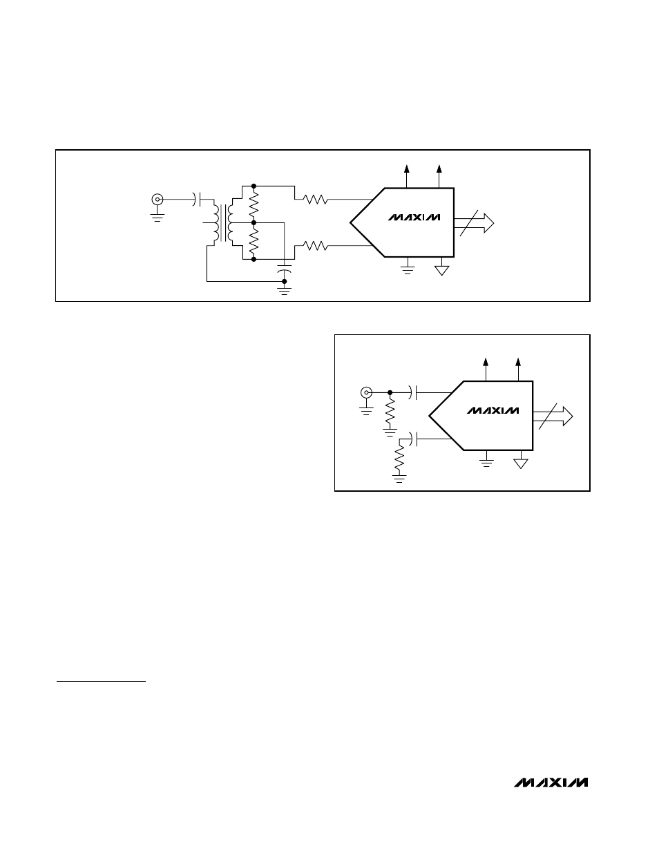
Figure 8 depicts a secondary-side termination of the 1:1
transformer into two separate 25Ω loads. Terminating
the transformer in this fashion reduces the potential
effects of transformer parasitics. The source impedance
combined with the shunt capacitance provided by a PC
board and the ADC’s parasitic capacitance reduce the
combined bandwidth to approximately 550MHz.
Single-Ended, AC-Coupled Analog Input
Although not recommended, the MAX1121 can be
used in single-ended mode (Figure 9). Analog signals
can be AC-coupled to the positive input INP through a
0.1µF capacitor and terminated with a 50Ω resistor to
AGND. The negative input should be 25Ω reverse-ter-
minated and AC grounded with a 0.1µF capacitor.
Grounding, Bypassing, and Board
Layout Considerations
The MAX1121 requires board layout design techniques
suitable for high-speed data converters. This ADC pro-
vides separate analog and digital power supplies. The
analog and digital supply voltage pins accept input
voltage ranges of 1.7V to 1.9V. Although both supply
types can be combined and supplied from one source,
it is recommended to use separate sources to cut down
on performance degradation caused by digital switch-
ing currents, which can couple into the analog supply
network. Isolate analog and digital supplies (AV
CC
and
OV
CC
) where they enter the PC board with separate
networks of ferrite beads and capacitors to their corre-
sponding grounds (AGND, OGND).
To achieve optimum performance, provide each supply
with a separate network of a 47µF tantalum capacitor in
parallel with 10µF and 1µF ceramic capacitors.
Additionally, the ADC requires each supply pin to be
bypassed with separate 0.1µF ceramic capacitors
(Figure 10). Locate these capacitors directly at the ADC
supply pins or as close as possible to the MAX1121.
Choose surface-mount capacitors, which are preferably
located on the same side as the converter, to save
space and minimize the inductance.
1.8V, 8-Bit, 250Msps Analog-to-Digital Converter
with LVDS Outputs for Wideband Applications
14
______________________________________________________________________________________
MAX1121
8
D0P/N–D7P/N
AV
CC
OV
CC
AGND
OGND
INP
INN
25Ω
25Ω
15Ω
15Ω
ADT1–1WT
0.1µF
0.1µF
SINGLE-ENDED
INPUT TERMINAL
Figure 8. Transformer-Coupled Analog Input Configuration with Secondary-Side Termination
MAX1121
8
D0P/N–D7P/N
AV
CC
OV
CC
AGND
OGND
0.1µF
SINGLE-ENDED
INPUT TERMINAL
0.1µF
INP
INN
50Ω
25Ω
Figure 9. Single-Ended AC-Coupled Analog Input
Configuration