Clock outputs (dclkp, dclkn) – Rainbow Electronics MAX1121 User Manual
Page 11
and are usually driven in AC-coupled configuration.
See the Differential, AC-Coupled Clock Input in the
Applications Information section for more circuit details
on how to drive CLKP and CLKN appropriately.
Although not recommended, the clock inputs also
accept a single-ended input signal.
The MAX1121 also features an internal clock manage-
ment circuit (duty-cycle equalizer) that ensures that the
clock signal applied to inputs CLKP and CLKN is
processed to provide a 50% duty cycle clock signal,
which desensitizes the performance of the converter to
variations in the duty cycle of the input clock source.
Note that the clock duty-cycle equalizer cannot be
turned off externally and requires a minimum clock fre-
quency of >20MHz to work appropriately and accord-
ing to data sheet specifications.
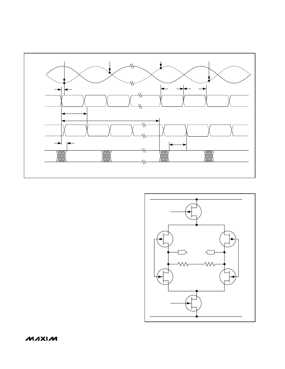
Clock Outputs (DCLKP, DCLKN)
The MAX1121 features a differential clock output, which
can be used to latch the digital output data with an
external latch or receiver. Additionally, the clock output
can be used to synchronize external devices (e.g.,
FPGAs) to the ADC. DCLKP and DCLKN are differential
outputs with LVDS-compatible voltage levels. There is a
2.1ns delay time between the rising (falling) edge of
CLKP (CLKN) and the rising edge of DCLKP (DCLKN).
See Figure 4 for timing details.
MAX1121
1.8V, 8-Bit, 250Msps Analog-to-Digital Converter
______________________________________________________________________________________
11
INP
INN
D0P/N–D7P/N
ORP/N
CLKP
CLKN
t
CH
t
CL
DCLKP
DCLKN
N - 8
N - 7
N
N + 1
t
PDL
N - 7
N - 8
N
N + 1
N
N + 1
N + 8
N + 9
t
CPDL
t
LATENCY
t
AD
N - 1
SAMPLING EVENT
SAMPLING EVENT
SAMPLING EVENT
SAMPLING EVENT
t
CPDL
- t
PDL
t
CPDL
- t
PDL
~ 0.4 x t
SAMPLE
with t
SAMPLE
= 1 / f
SAMPLE
NOTE: THE ADC SAMPLES ON THE RISING EDGE OF CLKP. THE RISING EDGE OF DCLKP CAN BE USED TO EXTERNALLY LATCH THE OUTPUT DATA.
Figure 4. System and Output Timing Diagram
OV
CC
OGND
2.2kΩ
2.2kΩ
V
OP
V
ON
Figure 5. Simplified LVDS Output Architecture