Applications information – Rainbow Electronics MAX1121 User Manual
Page 13
Applications Information
Full-Scale Range Adjustments Using the
Internal Bandgap Reference
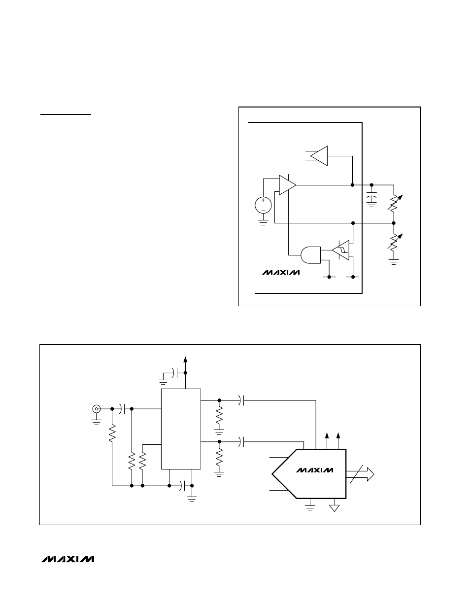
The MAX1121 supports a full-scale adjustment range of
10% (±5%). To decrease the full-scale range, an exter-
nal resistor value ranging from 13kΩ to 1MΩ may be
added between REFADJ and AGND. A similar
approach can be taken to increase the ADCs full-scale
range. Adding a variable resistor, potentiometer, or
predetermined resistor value between REFADJ and
REFIO increases the full-scale range of the data con-
verter. Figure 6 shows the two possible configurations
and their impact on the overall full-scale range adjust-
ment of the MAX1121. Do not use resistor values of less
than 13kΩ to avoid instability of the internal gain regula-
tion loop for the bandgap reference.
Differential, AC-Coupled, PECL-Compatible
Clock Input
The preferred method of clocking the MAX1121 is differ-
entially with LVDS- or PECL-compatible input levels. To
accomplish this, a 50Ω reverse-terminated clock signal
source with low phase noise is AC-coupled into a fast dif-
ferential receiver such as the MC100LVEL16 (Figure 7).
The receiver produces the necessary PECL output levels
to drive the clock inputs of the data converter.
MAX1121
1.8V, 8-Bit, 250Msps Analog-to-Digital Converter
with LVDS Outputs for Wideband Applications
______________________________________________________________________________________
13
REFERENCE
BUFFER
REFIO
REFADJ
AV
CC
AV
CC
/ 2
CONTROL LINE TO
DISABLE REFERENCE
BUFFER
ADC FULL-SCALE = REFT - REFB
G
1V
0.1µF
REFERENCE-
SCALING
AMPLIFIER
REFT
REFB
13kΩ
TO 1MΩ
13kΩ
TO 1MΩ
MAX1121
Figure 6. Circuit Suggestions to Adjust the ADC’s Full-Scale
Range
MAX1121
50Ω
CLKP
CLKN
SINGLE-ENDED
INPUT TERMINAL
MC100LVEL16
510Ω
510Ω
150Ω
150Ω
V
CLK
VGND
2
3
4
5
6
7
8
0.1µF
0.1µF
0.1µF
0.1µF
0.01µF
8
D0P/N–D7P/N
AV
CC
OV
CC
AGND
OGND
INP
INN
Figure 7. Differential, AC-Coupled, PECL-Compatible Clock Input Configuration