Pin description – Rainbow Electronics MAX1121 User Manual
Page 8
MAX1121
1.8V, 8-Bit, 250Msps Analog-to-Digital Converter
with LVDS Outputs for Wideband Applications
8
_______________________________________________________________________________________
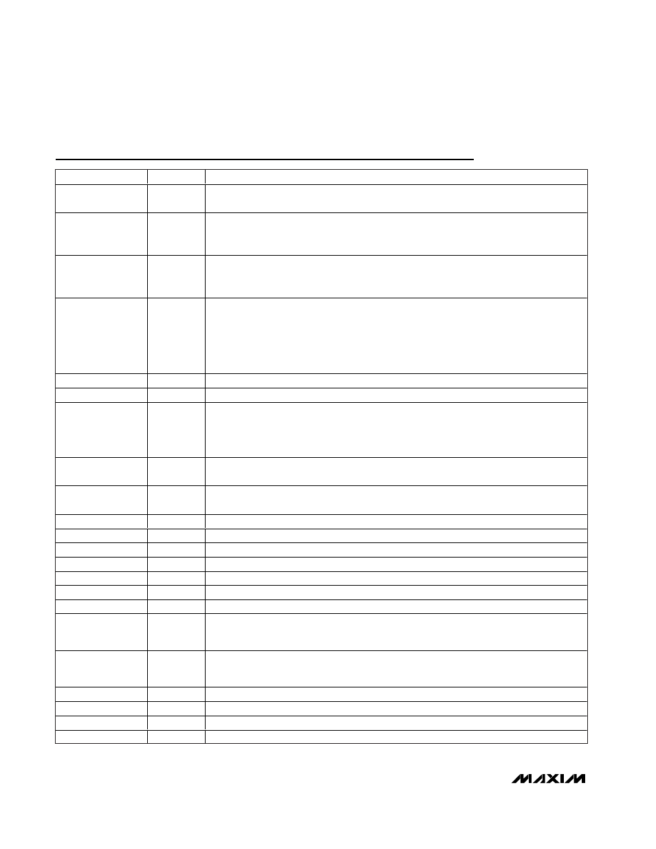
Pin Description
PIN
NAME
FUNCTION
1, 6, 11–14, 20,
25, 62, 63, 65
AV
CC
Analog Supply Voltage. Bypass each pin with a 0.1µF capacitor for best decoupling results.
2, 5, 7, 10, 15, 16,
18, 19, 21, 24, 64,
66, 67, EP
AGND
Analog Converter Ground. Connect the converter’s exposed paddle (EP) to AGND.
3
REFIO
Reference Input/Output. With REFADJ pulled high through a 1kΩ resistor, this I/O port allows
an external reference source to be connected to the MAX1121. With REFADJ pulled low
through the same 1kΩ resistor, the internal 1.23V bandgap reference is active.
4
REFADJ
Reference-Adjust Input. REFADJ allows for full-scale range adjustments by placing a resistor
or trim potentiometer between REFADJ and AGND (decreases FS range) or REFADJ and
REFIO (increases FS range). If REFADJ is connected to AV
CC
through a 1kΩ resistor, the
internal reference can be overdriven with an external source connected to REFIO. If REFADJ
is connected to AGND through a 1kΩ resistor, the internal reference is used to determine the
full-scale range of the data converter.
8
INP
Positive Analog Input Terminal
9
INN
Negative Analog Input Terminal
17
CLKDIV
Clock Divider Input. This LVCMOS-compatible input controls which speed the converter’s
digital outputs are updated. CLKDIV has an internal pulldown resistor.
CLKDIV = 0: ADC updates digital outputs at one-half the input clock rate.
CLKDIV = 1: ADC updates digital outputs at the input clock rate.
22
CLKP
True Clock Input. This input requires an LVDS-compatible input level to maintain the
converter’s excellent performance.
23
CLKN
Complementary Clock Input. This input requires an LVDS-compatible input level to maintain
the converter’s excellent performance.
26, 45, 61
OGND
Digital Converter Ground. Ground connection for digital circuitry and output drivers.
27, 28, 41, 44, 60
OV
CC
Digital Supply Voltage.
Bypass with a 0.1µF capacitor for best decoupling results.
29–36
N.C.
No Connection. Do not connect to these pins.
37
D0N
Complementary Output Bit 0 (LSB)
38
D0P
True Output Bit 0 (LSB)
39
D1N
Complementary Output Bit 1
40
D1P
True Output Bit 1
42
DCLKN
Complementary Clock Output. This output provides an LVDS-compatible output level and can
be used to synchronize external devices to the converter clock. There is a 2.1ns delay
between CLKN and DCLKN.
43
DCLKP
True Clock Output. This output provides an LVDS-compatible output level and can be used to
synchronize external devices to the converter clock. There is a 2.1ns delay between CLKP
and DCLKP.
46
D2N
Complementary Output Bit 2
47
D2P
True Output Bit 2
48
D3N
Complementary Output Bit 3
49
D3P
True Output Bit 3