Pin description – Rainbow Electronics MAX1427 User Manual
Page 8
MAX1427
15-Bit, 80Msps ADC with -79.3dBFS
Noise Floor for Baseband Applications
8
_______________________________________________________________________________________
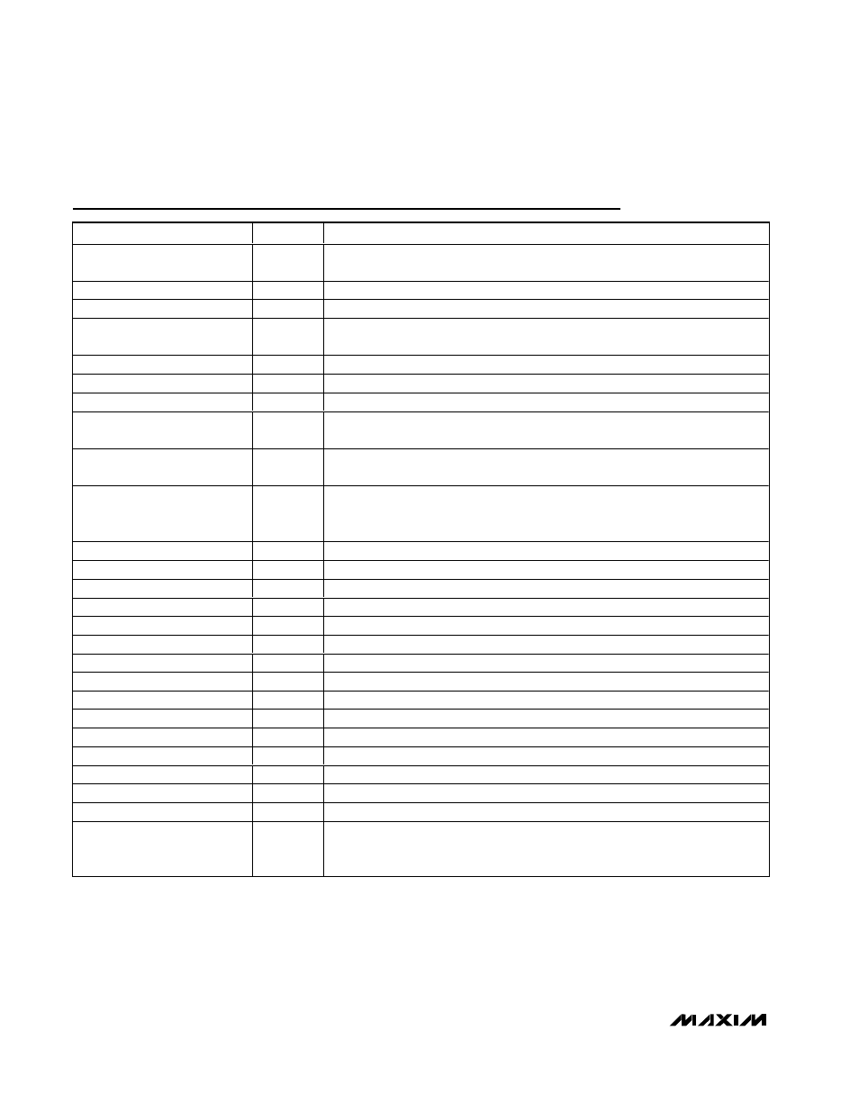
Pin Description
PIN
NAME
FUNCTION
1, 2, 3, 6, 9, 12, 14–17,
20, 23, 26, 27, 30, 52–56, EP
GND
Converter Ground. Analog, digital, and output driver grounds are internally
connected to the same potential. Connect the converter’s EP to GND.
4
CLKP
Differential Clock, Positive Input Terminal
5
CLKN
Differential Clock, Negative Input Terminal
7, 8, 18, 19, 21, 22, 24, 25, 28
AV
CC
Analog Supply Voltage. Provide local bypassing to ground with 0.1µF to 0.22µF
capacitors.
10
INP
Differential Analog Input, Positive Terminal
11
INN
Differential Analog Input, Negative/Complementary Terminal
13
CM
Common-Mode Reference Terminal
29
DV
CC
Digital Supply Voltage.
Provide local bypassing to ground with 0.1µF to 0.22µF
capacitors.
31, 41, 42, 51
DRV
CC
Digital Output Driver Supply Voltage. Provide local bypassing to ground with
0.1µF to 0.22µF capacitors.
32
DOR
Data Overrange Bit. This control line flags an overrange condition in the ADC.
If DOR transitions high, an overrange condition is detected. If DOR remains low, the
ADC operates within the allowable full-scale range.
33
D0
Digital CMOS Output Bit 0 (LSB)
34
D1
Digital CMOS Output Bit 1
35
D2
Digital CMOS Output Bit 2
36
D3
Digital CMOS Output Bit 3
37
D4
Digital CMOS Output Bit 4
38
D5
Digital CMOS Output Bit 5
39
D6
Digital CMOS Output Bit 6
40
D7
Digital CMOS Output Bit 7
43
D8
Digital CMOS Output Bit 8
44
D9
Digital CMOS Output Bit 9
45
D10
Digital CMOS Output Bit 10
46
D11
Digital CMOS Output Bit 11
47
D12
Digital CMOS Output Bit 12
48
D13
Digital CMOS Output Bit 13
49
D14
Digital CMOS Output Bit 14 (MSB)
50
DAV
Data Valid Output. This output can be used as a clock control line to drive an
external buffer or data-acquisition system. The typical delay time between the
falling edge of the converter clock and the rising edge of DAV is 6.5ns.