Rainbow Electronics MAX1427 User Manual
Page 14
MAX1427
15-Bit, 80Msps ADC with -79.3dBFS
Noise Floor for Baseband Applications
14
______________________________________________________________________________________
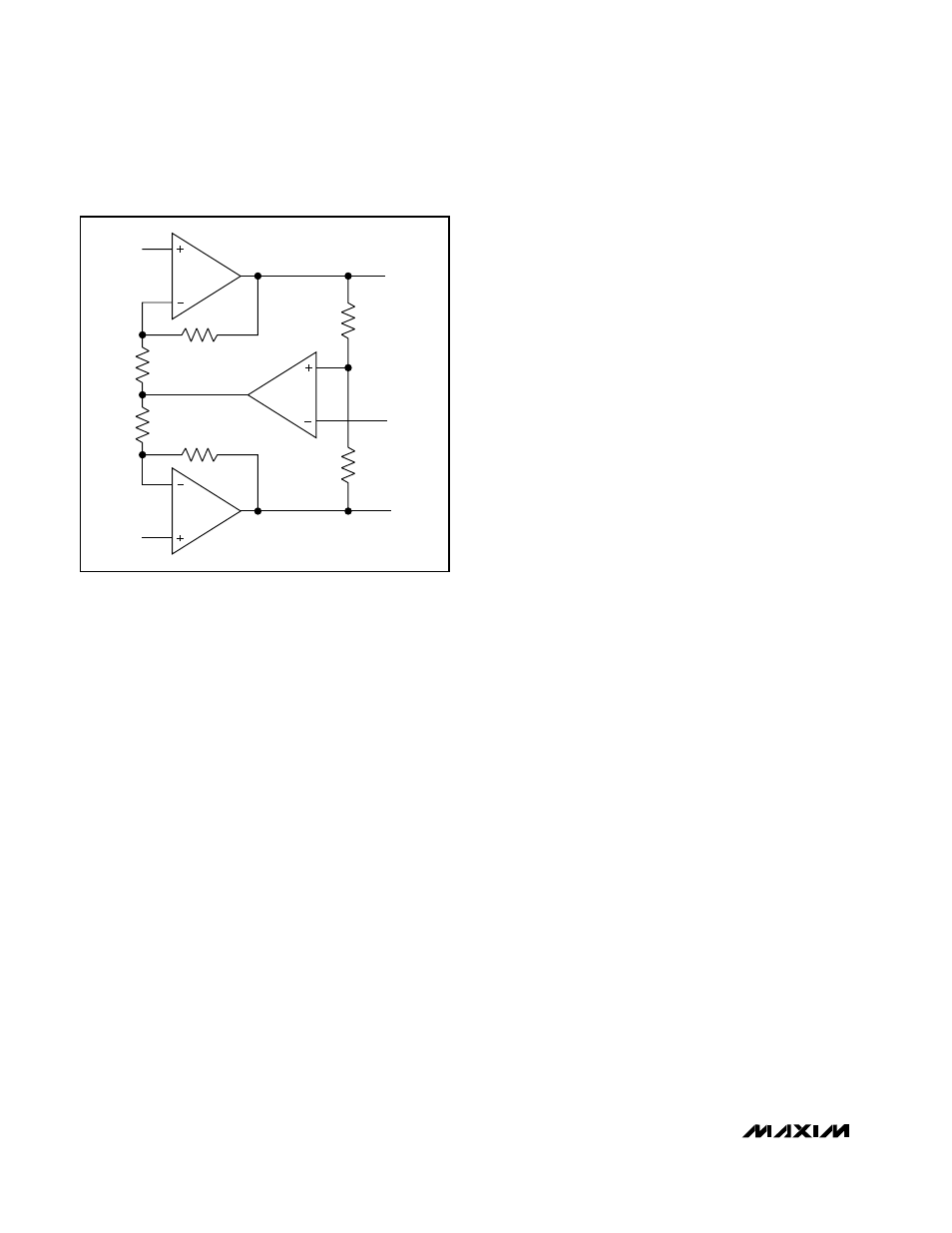
DC-Coupled Analog Input
While AC-coupling of the input signal is the proper
means for achieving the best dynamic performance, it
is possible to DC-couple the inputs by making use of
the CM potential. Figure 8 shows one method for
accomplishing DC-coupling. The common-mode
potentials at the outputs of amplifiers OA1 and OA2 are
“servoed” by the action of amplifier OA3 to be equal to
the CM potential of the MAX1427. Care must be taken
to ensure that the common-mode loop is stable, and
the R
F
/R
G
ratios of both half circuits must be well
matched to ensure balance.
PC Board Layout Considerations
The performance of any high-dynamic range, high
sample-rate converter may be compromised by poor
PC board layout practices. The MAX1427 is no excep-
tion to the rule, and careful layout techniques must be
observed in order to achieve the specified perfor-
mance. Layout issues are addressed in the following
four categories:
1) Layer assignments
2) Signal routing
3) Grounding
4) Supply routing and bypassing
The MAX1427 evaluation board (MAX1427 EV kit) pro-
vides an excellent frame of reference for board layout,
and the discussion that follows is consistent with the
practices incorporated on the evaluation board.
Layer Assignments
The MAX1427 EV kit is a six-layer board, and the
assignment of layers is discussed in this context. It is
recommended that the ground plane be on a layer
between the signal routing layer and the supply routing
layer(s). This practice prevents coupling from the sup-
ply lines into the signal lines. The MAX1427 EV kit PC
board places the signal lines on the top (component)
layer and the ground plane on layer 2. Any region on
the top layer not devoted to signal routing is filled with
ground plane with vias to layer 2. Layers 3 and 4 are
devoted to supply routing, layer 5 is another ground
plane, and layer 6 is used for the placement of addi-
tional components and for additional signal routing.
A four-layer implementation is also feasible using layer
1 for signal lines, layer 2 as a ground plane, layer 3 for
supply routing, and layer 4 for additional signal routing.
However, care must be taken to make sure that the
clock and signal lines are isolated from each other and
from the supply lines.
Signal Routing
In order to preserve good even-order distortion, the sig-
nal lines (those traces feeding the INP and INN inputs)
must be carefully balanced. To accomplish this, the sig-
nal traces should be made as symmetric as possible,
meaning that each of the two signal traces should be the
same length and should see the same parasitic environ-
ment. As mentioned previously, the signal lines must be
isolated from the supply lines to prevent coupling from
the supplies to the inputs. This is accomplished by mak-
ing the necessary layer assignments as described in the
previous section. Additionally, it is crucial that the clock
lines be isolated from the signal lines. On the MAX1427
EV kit, this is done by routing the clock lines on the bot-
tom layer (layer 6). The clock lines then connect to the
ADC through vias placed in close proximity to the
device. The clock lines are isolated from the supply lines,
by virtue of the ground plane on layer 5.
The digital output traces should be kept as short as
possible to minimize capacitive loading. The ground
plane on layer 2 beneath these traces should not be
removed so that the digital ground return currents have
an uninterrupted path back to the bypass capacitors.
FROM CM
TO INN
TO INP
OA1
OA2
OA3
R
C2
R
C1
R
G1
R
G2
POSITIVE
INPUT
NEGATIVE
INPUT
R
F1
R
F1
Figure 8. DC-Coupled Analog Input Configuration