Rainbow Electronics MAX1427 User Manual
Page 11
MAX1427
15-Bit, 80Msps ADC with -79.3dBFS
Noise Floor for Baseband Applications
______________________________________________________________________________________
11
• t
DGV
: Time from the rising edge of the clock until data
is guaranteed to be valid
• t
SETUP
: Time from data guaranteed valid until the ris-
ing edge of DAV
• t
HOLD
: Time from the rising edge of DAV until data is
no longer valid
• t
CLKP
: Time from the 50% point of the rising edge to
the 50% point of the falling edge of the clock signal
• t
CLKN
: Time from 50% point of the falling edge to the
50% point of the rising edge of the clock signal
The MAX1427 samples the input signal on the rising
edge of the input clock. Output data is valid on the ris-
ing edge of the DAV signal, with a data latency of three
clock cycles. Note that the clock duty cycle must be
50% ±5% for proper operation.
Digital Outputs (D0–D14, DAV, DOR)
The logic “high” level of the CMOS-compatible digital
outputs (D0–D14, DAV, and DOR) may be set in the
2.3V to 3.5V range. This is accomplished by setting the
voltage at the DV
CC
and DRV
CC
pins to the desired
logic-high level.
Note that the DV
CC
and DRV
CC
volt-
ages must be the same value.
For best performance, the capacitive loading on the digital
outputs of the MAX1427 should be kept as low as possible
(<10pF). Large capacitive loads result in large charging
currents during data transitions, which may feed back into
the analog section of the ADC and create distortion terms.
The loading capacitance is kept low by keeping the output
traces short and by driving a single CMOS buffer or latch
input (as opposed to multiple CMOS inputs).
Inserting small series resistors (220Ω or less) between
the MAX1427 outputs and the digital load, placed as
closely as possible to the output pins, is helpful in con-
trolling the size of the charging currents during data
transitions and can improve dynamic performance.
Keep the trace length from the resistor to the load as
short as possible to minimize trace capacitance.
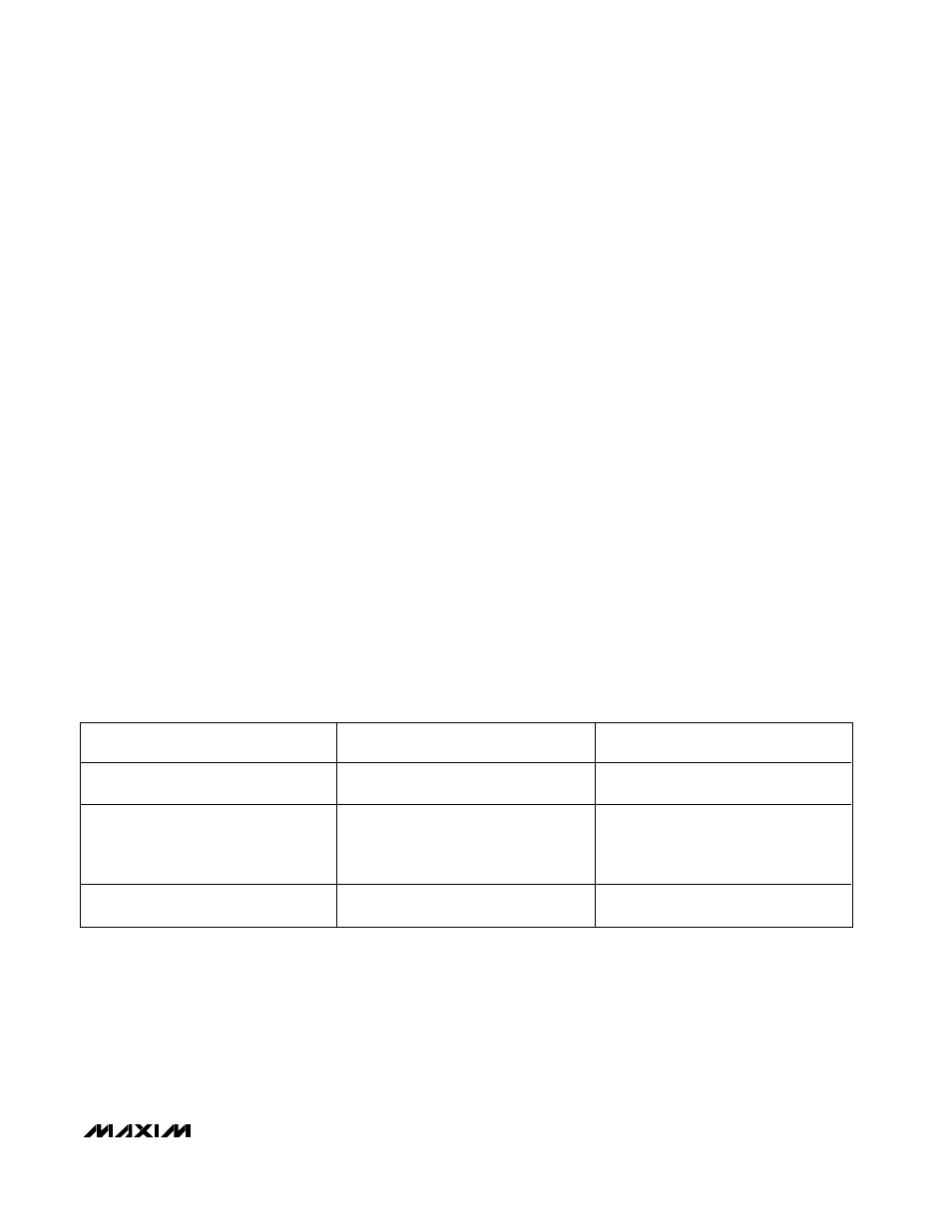
The output data is in two’s complement format, as illus-
trated in Table 1.
Data is valid at the rising edge of DAV (Figure 4), and
DAV may be used as a clock signal to latch the output
data. The DAV output provides twice the drive strength
of the data outputs, and may therefore be used to drive
multiple data latches.
The DOR output is used to identify an overrange condi-
tion. If the input signal exceeds the positive or negative
full-scale range for the MAX1427, then DOR is asserted
high. The timing for DOR is identical to the timing for
the data outputs, and DOR therefore provides an over-
range indication on a sample-by-sample basis.
Table
1. MAX1419 Digital Output Coding
INP
ANALOG VOLTAGE LEVEL
INN
ANALOG VOLTAGE LEVEL
D14–D0
TWO’S COMPLEMENT CODE
V
REF
+ 0.64V
V
REF
- 0.64V
0 1 1 1 1 1 1 1 1 1 1 1 1 1 1
(positive full scale)
V
REF
V
REF
0 0 0 0 0 0 0 0 0 0 0 0 0 0 0
(midscale +
δ
)
1 1 1 1 1 1 1 1 1 1 1 1 1 1 1
(midscale -
δ
)
V
REF
- 0.64V
V
REF
+ 0.64V
1 0 0 0 0 0 0 0 0 0 0 0 0 0 0
(negative full scale)