Electrical characteristics (continued) – Rainbow Electronics MAX1427 User Manual
Page 4
MAX1427
15-Bit, 80Msps ADC with -79.3dBFS
Noise Floor for Baseband Applications
4
_______________________________________________________________________________________
Note 1: Dynamic performance is based on a 32,768-point data record with a sampling frequency of f
SAMPLE
= 80.019456MHz, an
input frequency of f
IN
= f
SAMPLE
x (6143/32768) = 15.001206MHz, and a frequency bin size of 2442Hz. Close-in (f
IN
±29.3kHz) and low-frequency (DC to 58.6kHz) bins are excluded from the spectrum analysis.
Note 2: Apply the same voltage levels to DV
CC
and DRV
CC
.
Note 3: Guaranteed by design and characterization.
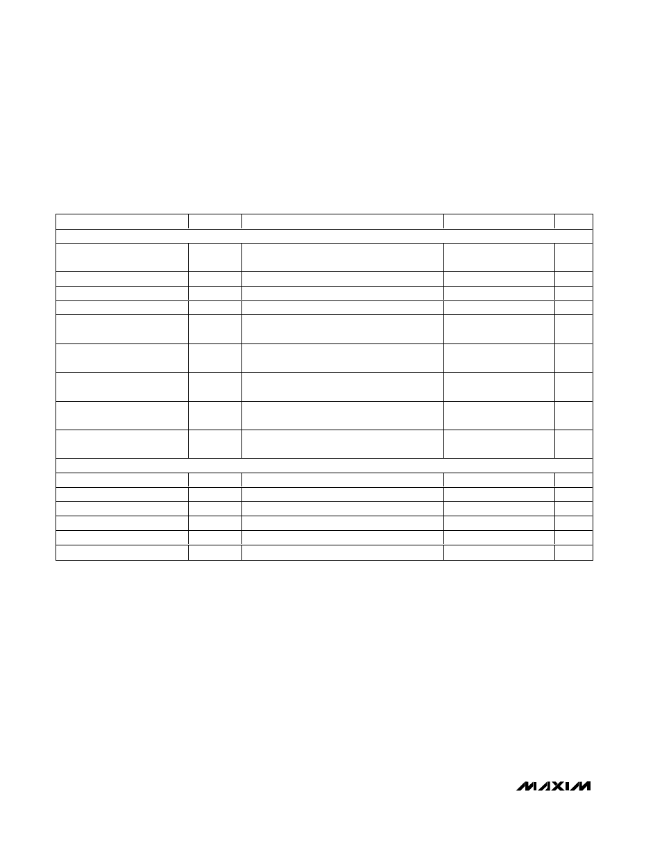
ELECTRICAL CHARACTERISTICS (continued)
(AV
CC
= 5V, DV
CC
= DRV
CC
= 2.5V, GND = 0, INP and INN driven differentially with -1dBFS, CLKP and CLKN driven differentially
with a 2V
P-P
sinusoidal input signal, C
L
= 5pF at digital outputs, f
CLK
= 80MHz, T
A
= T
MIN
to T
MAX
, unless otherwise noted. Typical
values are at T
A
= +25°C, unless otherwise noted. ≥+25°C guaranteed by production test, <+25°C guaranteed by design and char-
acterization.)
PARAMETER
SYMBOL
CONDITIONS
MIN
TYP
MAX
UNITS
TIMING CHARACTERISTICS (DV
CC
= DRV
CC
= 3.3V)
Figure
4
CLKP/CLKN Duty Cycle
Duty cycle
50
±5
%
Effective Aperture Delay
t
AD
230
ps
Output Data Delay
t
DAT
(Note 3)
2.8
4.1
6.5
ns
Data Valid Delay
t
DAV
(Note 3)
5.3
6.3
8.6
ns
Pipeline Latency
t
LATENCY
3
Clock
cycles
CLKP Rising Edge to
DATA Not Valid
t
DNV
(Note 3)
2.5
3.4
5.2
ns
CLKP Rising Edge to
DATA Valid (Guaranteed)
t
DGV
(Note 3)
3.2
4.4
7.4
ns
DATA Setup Time
(Before DAV Rising Edge)
t
SETUP
(Note 3)
t
CLKP
+ 0.2
t
CLKP
+ 1.7
t
CLKP
+ 2.8
ns
DATA Hold Time
(After DAV Rising Edge)
t
HOLD
(Note 3)
t
CLKN
-
3.5
t
CLKN
-
2.7
t
CLKN
-
2.0
ns
POWER REQUIREMENTS
Analog Supply Voltage Range
AV
CC
5 ±3%
V
Digital Supply Voltage Range
DV
CC
(Note 2)
2.3 to 3.5
V
Output Supply Voltage Range
DRV
CC
(Note 2)
2.3 to 3.5
V
Analog Supply Current
I
AVCC
377
440
mA
D i g i tal + Outp ut S up p l y C ur r ent
I
DVCC
+
f
CLK
= 80MHz, C
LOAD
= 5pF
35.5
42
mA
Analog Power Dissipation
PDISS
1974
mW